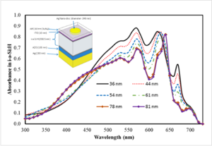
Recent numerical modeling of plasmonic metallic nanostructures have shown great potential as a method of light management in thin-film nanodisc-patterned hydrogenated amorphous silicon (a-Si:H) solar photovoltaic (PV) cells. A significant design challenge for such plasmonic-enhanced PV devices is the requirement for ultra-thin transparent conducting oxides (TCOs) with high transmittance (low loss) and low enough resistivity to be used as device top contacts/electrodes. Most work on TCOs is on relatively thick layers and the few reported cases of thin TCO showed a marked decrease in conductivity. Recent work on ultra-thin TCOs of aluminum-doped zinc oxide, indium-doped tin oxide and zinc oxide revealed an unavoidable trade-off between transmittance and resistivity when fabricated with conventional growth methods. Ultra-thin films showed a tendency to be either amorphous and continuous or form as isolated islands. This results in poor electrical properties, which cannot be improved with annealing as the delicate thin films nucleate to form grain clusters. In order to overcome this challenge, this study investigates a novel method of producing ultra-thin (<40 nm) high quality TCOs. First, ~80 nm ITO films are sputtered in various argon–oxygen atmospheres and annealed to increase conductivity. The most promising materials were then reduced in thickness with a controlled low-cost room-temperature cyclic wet chemical etching process to reach the desired thickness. The degradation in the electrical conductivity was tracked as a function of thickness. The sheet resistance of 36 nm thin films was observed to be of the same order compared to the much thicker commercial ITO films currently used as transparent electrodes in PV and other opto-electronic devices. Experimental optical properties of the shaved films were then used in an optimized model of nano-disc plasmonic a-Si:H solar cells. Simulations indicate that optical enhancement greater than 21% are possible in the 300–730 nm wavelength range, when compared to the reference cell. Using the novel chemical shaving method described here, high-quality ultra-thin ITO films capable of improving the efficiency of thin film a-Si:H solar cells have been demonstrated. The methods employed in the optimization process are well established and economically viable, which provide the technical potential for commercialization of plasmonic based solar cells.
Keywords[edit | edit source]
Transparent conducting oxide; Indium tin oxide; Plasmonic; Amorphous silicon; Optical enhancement;photovoltaics; optics
Highlights[edit | edit source]
- Plasmonic metallic nanostructures potential in a-Si:H PV light management.
- Work to date shows a marked decrease in conductivity as thickness decreases.
- Here ultra-thin (<40 nm) high quality TCOs fabricated, tested simulated.
- 80 nm ITO films are sputtered, annealed, controlled cyclic wet chemical etch.
- 36 nm thin films with optical enhancement greater than 21% (300–730 nm).
See also[edit | edit source]
- Influence of Oxygen Concentration on the Performance of Ultra-Thin RF Magnetron Sputter Deposited Indium Tin Oxide Films as a Top Electrode for Photovoltaic Devices
- Limitations of ultra-thin transparent conducting oxides for integration into plasmonic-enhanced thin-film solar photovoltaic devices
- Advances in plasmonic light trapping in thin-film solar photovoltaic devices
- Controlling optical absorption in metamaterial absorbers for plasmonic solar cells
- Plasmonic Perfect Meta-Absobers for a-Si PV Devices
- Plasmonic enhancement of amorphous silicon solar photovoltaic cells with hexagonal silver arrays made with nanosphere lithography
- Optical modelling of thin film microstructures literature review
- Multi-resonant silver nano-disk patterned thin film hydrogenated amorphous silicon solar cells for Staebler-Wronski effect compensation
- Effect of ambient combinations of argon, oxygen, and hydrogen on the properties of DC magnetron sputtered indium tin oxide films
- A novel synthesis of tin oxide thin films by the sol-gel process for optoelectronic applications
- Enhancement of hydrogenated amorphous silicon solar cells with front-surface hexagonal plasmonic arrays from nanoscale lithography
- Fabricating Ordered 2-D Nano-Structured Arrays Using Nanosphere Lithography
- Ambiance-dependent Agglomeration and Surface-enhanced Raman Spectroscopy Response of Self-assembled Silver Nano-particles for Plasmonic Photovoltaic Devices
- Micromorphology analysis of sputtered indium tin oxide fabricated with variable ambient combinations
- Properties of Al-Doped Zinc Oxide and In-Doped Zinc Oxide Bilayer Transparent Conducting Oxides for Solar Cell Applications
- Optimal Design of Thin-film Plasmonic Solar Cells using Differential Evolution Optimization Algorithms
- MACE nano-texture process applicable for both single- and multi-crystalline diamond-wire sawn Si solar cells
- Scalable honeycomb top contact to increase the light absorption and reduce the series resistance of thin film solar cells
- Influence of metal assisted chemical etching time period on mesoporous structure in as-cut upgraded metallurgical grade silicon for solar cell application
- Optoelectronic Properties: Carrier Transport, Recombination, and Stability


