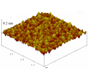
The opportunity for substantial efficiency enhancements of thin film hydrogenated amorphous silicon (a-Si:H) solar photovoltaic (PV) cells using plasmonic absorbers requires ultra-thin transparent conducting oxide top electrodes with low resistivity and high transmittances in the visible range of the electromagnetic spectrum. Fabricating ultra-thin indium tin oxide (ITO) films (sub-50 nm) using conventional methods has presented a number of challenges; however, a novel method involving chemical shaving of thicker (greater than 80 nm) RF sputter deposited high-quality ITO films has been demonstrated. This study investigates the effect of oxygen concentration on the etch rates of RF sputter deposited ITO films to provide a detailed understanding of the interaction of all critical experimental parameters to help create even thinner layers to allow for more finely tune plasmonic resonances. ITO films were deposited on silicon substrates with a 98-nm, thermally grown oxide using RF magnetron sputtering with oxygen concentrations of 0, 0.4 and 1.0 sccm and annealed at 300 °C air ambient. Then the films were etched using a combination of water and hydrochloric and nitric acids for 1, 3, 5 and 8 min at room temperature. In-between each etching process cycle, the films were characterized by X-ray diffraction, atomic force microscopy, Raman Spectroscopy, 4-point probe (electrical conductivity), and variable angle spectroscopic ellipsometry. All the films were polycrystalline in nature and highly oriented along the (222) reflection. Ultra-thin ITO films with record low resistivity values (as low as 5.83 × 10⁻⁴ Ω·cm) were obtained and high optical transparency is exhibited in the 300–1000 nm wavelength region for all the ITO films. The etch rate, preferred crystal lattice growth plane, d-spacing and lattice distortion were also observed to be highly dependent on the nature of growth environment for RF sputter deposited ITO films. The structural, electrical, and optical properties of the ITO films are discussed with respect to the oxygen ambient nature and etching time in detail to provide guidance for plasmonic enhanced a-Si:H solar PV cell fabrication.
Keywords[edit | edit source]
transparent conducting oxide; indium tin oxide; plasmonics; wet etching; photovoltaics; optics
See also[edit | edit source]
- Limitations of ultra-thin transparent conducting oxides for integration into plasmonic-enhanced thin-film solar photovoltaic devices
- A new method of preparing highly conductive ultra-thin indium tin oxide for plasmonic-enhanced thin film solar photovoltaic devices
- Advances in plasmonic light trapping in thin-film solar photovoltaic devices
- Controlling optical absorption in metamaterial absorbers for plasmonic solar cells
- Plasmonic Perfect Meta-Absobers for a-Si PV Devices
- Optical modelling of thin film microstructures literature review
- Multi-resonant silver nano-disk patterned thin film hydrogenated amorphous silicon solar cells for Staebler-Wronski effect compensation
- Effect of ambient combinations of argon, oxygen, and hydrogen on the properties of DC magnetron sputtered indium tin oxide films
- A novel synthesis of tin oxide thin films by the sol-gel process for optoelectronic applications
- Plasmonic enhancement of amorphous silicon solar photovoltaic cells with hexagonal silver arrays made with nanosphere lithography
- Enhancement of hydrogenated amorphous silicon solar cells with front-surface hexagonal plasmonic arrays from nanoscale lithography
- Fabricating Ordered 2-D Nano-Structured Arrays Using Nanosphere Lithography
- Ambiance-dependent Agglomeration and Surface-enhanced Raman Spectroscopy Response of Self-assembled Silver Nano-particles for Plasmonic Photovoltaic Devices
- Micromorphology analysis of sputtered indium tin oxide fabricated with variable ambient combinations
- Properties of Al-Doped Zinc Oxide and In-Doped Zinc Oxide Bilayer Transparent Conducting Oxides for Solar Cell Applications
- Optimal Design of Thin-film Plasmonic Solar Cells using Differential Evolution Optimization Algorithms
- Scalable honeycomb top contact to increase the light absorption and reduce the series resistance of thin film solar cells
- Optoelectronic Properties: Carrier Transport, Recombination, and Stability


