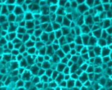
The size effect of nanoscale silicon in both amorphous and porous silicon was investigated with micro-Raman spectroscopy. Silicon nanostructures in amorphous silicon were deposited on quartz substrates by plasma enhanced chemical vapor deposition (PECVD) with deposition powers of 15, 30 and 50 W. Micro-Raman spectra of the nanostructured silicon show the T2g Raman active mode shifting from the 521 cm−1 crystalline Si Raman line to 494, 499 and 504 cm−1 as deposition power increased. Large Raman mode shifts, up to 27 cm−1 and broadening up to 23 cm−1 of the T2g Raman-active mode is attributed to a phonon confinement effect. The analysis of micro-Raman scattering data is useful to understand the role of deposition condition of the silicon sample. In addition, micro-Raman scattering intensity of porous silicon prepared using various current densities such as 10, 50 and 125 mA/cm2 has also been investigated. The effect of phonon confinement on the nanoscale porous silicon has been quantified. The relationship between Raman shift and stress on the porous silicon has been evaluated.
Keywords[edit | edit source]
amorphous silicon; micro-Raman; porous silicon; Raman shift and stress; scattering


