Designer
Juha Heinonen' Aalto University, Department of Electronics and Nanoengineering
Project
Silicon photodiodes are very sensitive devices that can be used to measure light with various wavelengths. However, the bare silicon chips are prone to damage and dirt that can affect their sensitivity. Additionally, connecting the chips to external cicuits is often not directly possible. Usually these problems are solved by attaching the chip to a circuit board and then sealing the board into a package which consists of a glass window and a frame made out of metal, plastic, or ceramic. In black silicon photodiodes researched by the Electron Physics Group of Aalto University, the problems with damage and dirt are even more severe. The nanostructured black silicon surface is very fragile and even small force can damage it. This also makes cleaning of the surface extremely difficult. Thus, some sort of protective package is urgently needed in order to keep the devices unharmed after their fabrication.
Fabricating the packages used in commercial photodiodes require sophisticated tools that can cost hundreds of thousands of dollars. There are also companies like Kyocera who offer manufacturing services. However, the tooling costs for a custom package design can be tens of thousnads of dollars which is too expensive for university researchers. The goal of this project is to design a similar photodiode package that could be fabricated with a 3D printer and thus avoiding the huge tool costs. A fully parametrized OpenSCAD code is designed which allows easy fabrication of packages for any sized photodiodes and windows.
This project was performed as a final project of the L3999 course Fall 2017.
Concept
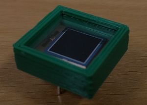
The designed photodiode package consists of a 3D-printed frame, a glass window and a PCB-board where the photodiode is attached. Before printig, the glass needs to be cut into right size, the PCB-board fabricated, and photodiode attached to it. All the design files can be found in the NIH printing respoitory. The demonstrated prototype was made for 12 x 12 mm photodiode chips and 18 x 18 mm glass window with 0.7 mm thickness. The included PCB-board design is for a 1.6 mm thick 18 x 18 mm board and three pins need to be soldered to it as contact legs. The printig is done in three steps explained in the instructions section so that the glass and PCB-board get embedded inside the frame and are thus firmly attached to it. An example gcode of the current design is included to demostrate how the printing can be paused to allow adding the parts into the frame.
Bill of Materials
- 3D-printed package frame
- 1 photodiode chip
- 1 custom PCB-board
- 3 connector pins
- 1 Glass window
Estimated Costs
- Printed parts $0.025/package (1 g PLA used according to Cura, PLA reel $25/kg)
- Contact pins $0.11/package (20 pins costs $0.766, 3 needed for each package)
- Glass window $0.98/package (6" borosilicate wafer $32.5/piece ~33 windows/wafer)
- PCB-board $0.27/package (100 x 160 mm blank PCB-board $11.04, 40 boards/piece)
- Total $1.385/package
Esitmation does not include any costs from PCB manufacturing, glass cutting, or chip attachment.
Directions
1) Download the design files from the NIH printing repository. If modifications to the design are needed (e.g. PCB-board or glass window with different size), change the parameters found at the beginning of the OpenSCAD code. After modifications, export STL-file.
2) Import STL-file into a slicing program to generate gcode. With the slicing program or directly in the gcode, find the layer where window and PCB slot sealing starts. Add pause command to the gcode before the sealing layer printing begins (at the beginnnig of layers 8 and 31 in the example code).
3) Fabricate the PCB board. Glue the photodiode chip to the large center metal pad with conductive epoxy and wire bond anode and guard ring to the smaller metal pads. The anode pad is marked AN and guard ring pad GR on the PCB-board.
4) Cut a proper sized glass window if it is not the correct size already.
5) Start the printing.
6) When the printer raises the print head, pauses, and the screen is saying "Waiting for user", insert the glass window in the formed slot of the frame. Make sure the glass is properly in the slot and that the glass edge is not higher than the frame walls.
7) Press the navigation button of the printer and the printing will continue.
8) When the print head is raised again and printing pauses, put the PCB-board on the formed slot upside down (detector chip towards the print bed). Make sure it is properly in the slot and that the board edge is not higher than the frame walls.
9) Press the printer navigation button to continue printing and wait it to finish.
10) Solder the contact pins to the holes on the exposed part of the backside of the PCB-board.
Planned upgrades
- Double sided PCB-board (already designed) which allows pins to be soldered afterwards. In the current protoype, the board was single sided which means that pins need to be soldered before printing which can cause the print head to collide with the pins and knock the package off the print bed.
- Explore other printing materials.
- Optimize the dimensions of the PCB-board and package to make it smaller.
- Test different window materials.
Parts
Images of finished parts
Package was printed using LulzBot TAZ 6 and PolyLite PLA was used as printing material. Print speed was 50 mm/s and layer height was 0.18 mm.


