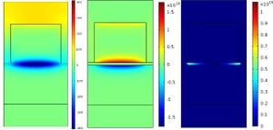
Using metamaterial absorbers, we have shown that metallic layers in the absorbers do not necessarily constitute undesired resistive heating problem for photovoltaics. Tailoring the geometric skin depth of metals and employing the natural bulk absorbance characteristics of the semiconductors in those absorbers can enable the exchange of undesired resistive losses with the useful optical absorbance in the active semiconductors. Thus, Ohmic loss dominated metamaterial absorbers can be converted into photovoltaic near-perfect absorbers with the advantage of harvesting the full potential of light management offered by the metamaterial absorbers. Based on experimental permittivity data for indium gallium nitride, we have shown that between 75%-95% absorbance can be achieved in the semiconductor layers of the converted metamaterial absorbers. Besides other metamaterial and plasmonic devices, our results may also apply to photodectors and other metal or semiconductor based optical devices where resistive losses and power consumption are important pertaining to the device performance.
See also[edit | edit source]
- Advances in plasmonic light trapping in thin-film solar photovoltaic devices
- Plasmonic Perfect Meta-Absobers for a-Si PV Devices
- Optical modelling of thin film microstructures literature review
- Multi-resonant silver nano-disk patterned thin film hydrogenated amorphous silicon solar cells for Staebler-Wronski effect compensation
- Effect of ambient combinations of argon, oxygen, and hydrogen on the properties of DC magnetron sputtered indium tin oxide films

