There is a page named "Semiconductor" on Appropedia. See also the other search results found.
- gallium arsenide solar cells Wikipedia:Semiconductor174 bytes (5 words) - 16:30, 1 June 2023
- Fabrication-based 3-D Printed Components with Solutions Commonly Used in Semiconductor Wet Processing Fused Particle Fabrication 3-D Printing: Recycled Materials'3 KB (381 words) - 13:38, 6 September 2024
- publications in industrial symbiosis Semiconductor recycling plant case study of CIGS photovoltaic manufacturing Semiconductor recycling plant case study of CIS5 KB (767 words) - 13:50, 23 October 2023
- printed devices in cleanroom environments for semiconductor processing. Materials Science in Semiconductor Processing 89 (2019), pp. 59-67. https://doi54 KB (5,723 words) - 10:07, 24 August 2024
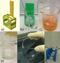
- with solvents, acids, bases and solutions used in the wet processing of semiconductor materials is explored. The results provide data on materials unavailable6 KB (600 words) - 19:41, 16 April 2024
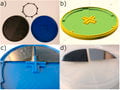
- for the wafer box 3-D printing, semiconductor wet processing, custom labware, clean rooms, Cleanroom, Silicon, Semiconductor processing, Polymers, Particle5 KB (558 words) - 15:59, 23 February 2024
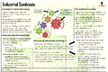
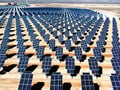
- factory a) greenhouse or b) mushroom growroom the photovoltaic plant semiconductor recycling plant Aluminum factory Packaging plant Cardboard factory The4 KB (3,571 words) - 18:20, 9 June 2023
- state lighting, electrons and holes are injected into a forward-biased semiconductor p-n junction; they recombine creating photons; the resulting photons4 KB (494 words) - 18:16, 13 June 2024
- A light-emitting diode (LED) is a semiconductor device that emits incoherent narrow-spectrum light when a p-n junction is forward electrically biased.12 KB (1,554 words) - 13:16, 9 June 2023
- important to ensure absorption of the entire solar spectrum while reducing semiconductor absorber layer thicknesses, which reduces deposition time, material use4 KB (430 words) - 16:00, 18 June 2024
- Gallium arsenide is a semiconductor with a greater saturated electron velocity and electron mobility than that of siliconW. A semiconductor is a material that23 KB (3,590 words) - 17:33, 27 June 2024
- (InGaN) is a III-N type semiconductor material, meaning elements from group III are combined with nitrogen to produce a semiconductor, that is gaining ground26 KB (3,519 words) - 12:23, 19 September 2024
- InGaN misc literature Review (section Engineering light absorption in semiconductor nanowire devices)has enabled a true revolution in the development of high-performance semiconductor materials and devices. Harnessing these powerful physical effects relies14 KB (1,867 words) - 13:39, 9 June 2023
- environments such as semiconductor processing systems and space environments. 3-D printing,chemical compatibility, semiconductor wet processing, custom3 KB (318 words) - 15:59, 23 February 2024
- Fabrication-based 3-D Printed Components with Solutions Commonly Used in Semiconductor Wet Processing 3-D Printable Polymer Pelletizer Chopper for Fused Granular4 KB (489 words) - 15:55, 23 February 2024
- the active semiconductors of the photovoltaic device. Considering experimental permittivity data for InxGa1-xN, absorbance in the semiconductor layers of3 KB (288 words) - 19:01, 16 April 2024
- syringe pump to form an additive manufacturing platform for thin film semiconductor devices. The full design of the slot die system is disclosed here using5 KB (559 words) - 06:23, 13 September 2024
- with a vision for semiconductor memory products. By 1971, they had introduced the world's first microprocessor. Type of Semiconductor and How it's Made24 KB (3,036 words) - 14:24, 6 July 2024
- consisting of semiconductor-insulator-semiconductor (SIS) heterojunction using surface plasmon polaritons (SPPs) generated in one of the semiconductors (Al:ZnO)171 KB (23,773 words) - 02:41, 1 June 2024
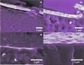
- damaged layer of semiconductors from sawing and to polish the semiconductor. As a result of processing, nearly 50% of the semiconductor is wasted. Thin30 KB (4,343 words) - 14:25, 28 February 2024