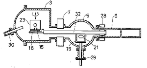
Molecular Beam Epitaxy (MBE) is a material fabrication process used to produce high-purity nano-scale materials. A material is grown through interactions between a substrate and one or more beams of atoms or molecules incident upon the substrate's surface. The beams are generated by sublimation of a solid source material. The entire process is performed under ultra high vacuumW. MBE exhibits many advantages over similar thin film deposition processes, like vapour deposition. Some of these advantages are: significantly improved purity, arbitrarily sharp deposition resolution, and operation at low temperatures.
System Description[edit | edit source]
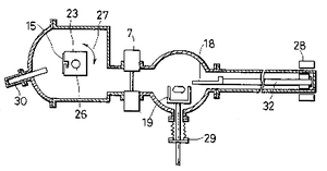
The main MBE apparatus is composed of two major sections: the substrate chamber and the effusion cells. All sections must be evacuated to low pressures to ensure that the molecular beam condition is achieved. This condition requires that the free path of a particle be greater than the dimensions of the substrate chamber. For a typical MBE set up, a pressure of 10E-4 Torr is sufficient, but pressures on the order of 10E-10 Torr are commonly used.[1]
Effusion Cells[edit | edit source]
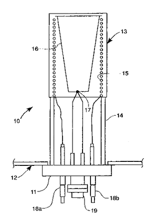
The effusion cells are the source of the molecular beams. A source material is placed in a crucible within the cells and heated by radiation from a resistive heating source. The solid source material sublimates due to the increased temperature and high vacuum. The pressure of the vapour can be controlled by varying the temperature of the solid phase, which in turn is controlled by variations in crucible heating. Because the beam intensity within the substrate chamber depends on the effusion cell pressures, the amount of material reaching the surface can be controlled by varying the source temperature.
Substrate Stage[edit | edit source]
A schematic of a basic substrate chamber is shown >. The effusion cells are attached to the chamber and oriented so as to direct the beam upon the substrate holder. The substrate holder is heated with a resistive element, as in the effusion cells.
The substrate is the material that the film will grow on. Common substrate materials are silicon, GaAs, and sapphire, but other substrates can be used. The choice of substrate is very important, and has been shown to effect the thin film microstructure. In fact, certain crystal structures have been found to be accessible only through a careful consideration of substrate behaviour.[2] The substrate stage can be rotated during deposition to increase the surface homogeneity.
Shutters[edit | edit source]
The shutters at the end of the collimation tunnel enable an operator to terminate the material flux from each cell separately. The shutter closing time is significantly smaller than a single layer deposition time. This means that the composition of the final material can be controlled at the monolayer level.
The orientation of the shutters relative to the beam direction is important for predictable operation of the system. Traditional shuttering systems had the shutters at right angles to the beam direction, directly blocking the beam path and redirecting some of the beam into the effusion cell. However, this method was found to adversely effect the beam flux continuity.[3] Variations of up to 20% in the beam flux following shutter opening and closing were observed, with a decay time of 30s. These variations can severely alter the composition of the growth material. It is now suggested that the shutters be placed some distance away from the effusion cells and at an angle, so that the beam is simply directed away from the substrate stage, as opposed to returned into the effusion cell. Any beam that hits the chamber wall is captured, so this process decreases materials efficiency as more is wasted, but increases reproducibility and control over the system. The balance between these two is application specific and must be taken into account.
RHEED[edit | edit source]
A RHEED (reflection high energy electron diffraction) monitoring system is implemented in modern MBE equipment. The RHEED system is used to monitor the growth surface during deposition. High energy electrons are incident upon the surface, producing a diffraction pattern upon the RHEED screen. The diffraction pattern can be analyzed to determine surface characteristics, like the material structure, as well as composition. The intensity of the diffraction pattern has been found to vary predictably with the surface layer formation, and can be used to determine when a monolayer has been fully formed. This information can be used to control the effusion cell shutters to produce an atomically flat surface.[1]
One further benefit of the RHEED apparatus is that it allows the operator to investigate the surface without requiring a direct view of the surface. This avoids the problems associated with viewing screens on UHV equipment.[4]
Principles of Operation[edit | edit source]
Molecular beam epitaxy is a complicated process. An understanding of how and why it works, however, can be had merely by understanding the basic materials engineering principles that underlie the process. There are two major topics within materials science that drive the MBE process: phase equilibrium within the effusion cells, and surface diffusion at the growth surface.
Phase equilibrium[edit | edit source]
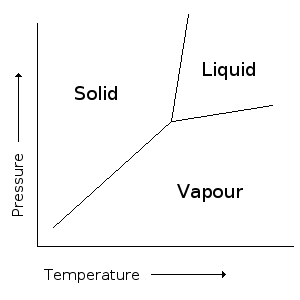
Within the effusion cells, the major process driving flux generation is the solid-vapour phase equilibriumW. A general phase diagram for a single component system is shown to the right. The pressure at which the MBE process is undertaken is below the triple point (where the three lines meet), and thus the only phases present at equilibrium are solid and vapour. Equilibrium is met at normal operating conditions if the effusion cell is properly designed. Gibb's phase law states
F = N +2 – P
Where F is the number of degrees of freedom of a system, N is the number of chemical components present, and P is the number of phases present.[5] In the effusion cell, there is one chemical component and two phases. Thus, there is only one degree of freedom, meaning that pressure and temperature cannot be changed independently. Conversely, this means that the pressure of the cell can be controlled by altering the temperature. The temperature and pressure are exponentially related, that is , where is the latent heat of vaporisation and is some constant that is independent of temperature.[1]
Surface Diffusion[edit | edit source]
As the material grows upon the substrate, the rate and type of crystal growthW are controlled by the energy available to the atoms. The diffusionW constant at the surface is given by:
Where is the surface diffusion coefficient, is the pre-exponential factor, Q is the activation energy, T is the temperature (in Kelvin) and k is Boltzmann's constant.[5]
The rate of surface diffusion is generally greater than that of bulk lattice diffusion. However, the surface area of a typical material is several orders of magnitude smaller than the bulk, and so is often ignored in diffusion considerations. During MBE growth, however, a very significant portion of the crystal is affected by its proximity to the surface. A greater amount of surface diffusion increases the rate of growth, as well as the surface quality. If atoms arriving can travel farther along the surface, they are more likely to arrive at the lowest energy, defect-free, state. Although limiting defects is energetically favoured, due to its lowering of surface energies, defect formation is favoured by entropic considerations. To overcome this, the surface area must be heated sufficiently so that the thermal energy of the diffusing atoms is great enough to diffuse out defects.
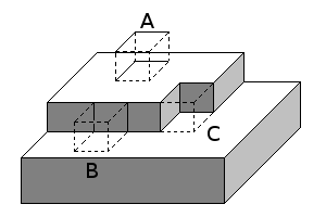
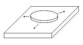
Minimization of surface energy is a major driving force for growth in MBE. When a single atom arrives on the surface, the total number of broken atomic bonds associated with the surface, in other words, its energy, increases. This atom on its own is unfavoured to remain on the surface, and is likely to return to the vapour phase after diffusing along the surface. If another atom should arrive nearby, and the two interact while diffusing, the number of broken bonds associated with the two atoms is decreased. The addition of a third atom leads to a further decrease in surface energy. This leads to the formation of "islands" of material on the surface. As more and more atoms arrive near the island, they tend toward the island, resulting in further island growth.
Atoms that arrive on top of the island will tend to diffuse off the island over a ledge. This jump down is energetically favoured. The number of broken bonds associated with the atom on top of the island is greater than that of an atom on the edge. Similarly, atoms will diffuse toward kinks in the ledge as opposed to open regions. No additional broken bonds are associated with joining the kink, whereas the formation of a new section of ledge involves the creation of many new broken bonds. This results in the growth of relatively circular islands. Due to the slow rate of growth in typical MBE applications, the rate of diffusion across the surface is great enough that atoms landing on top of an island on an incomplete layer will diffuse across the island, joining the incomplete layer.
Vacuum Considerations[edit | edit source]
The two biggest reasons for UHV within MBE are the demand for the beam condition and the minimization of contaminants in the atmosphere. The beam condition is met if the pressure is below 10^-4 Torr. Surface contaminant concentrations at this pressure, however, are unsuitable for high purity epitaxial growth. The rate at which vapour particles interact with a surface is given by:
Where dn/dt is the number of interactions per unit time per unit area, P is the pressure, m is the particle mass, T is temperature and k is Boltzmann's constant.[3] If P is taken in Torr, and m is replaced by M, the molar mass, the second expression is obtained. In standard atmospheric conditions, at a temperature of 25 degrees Celsius and an average vapour molar mass of 40g, the rate of interaction is linearly proportional to the pressure, as Torr. If, for example, the pressure is 10^-6 Torr (less than one thousandth of an atmosphere), the interaction rate is cm^-2 s^-1. As a guide, the surface atomic density of pure silicon is cm^-2. This means that, under these conditions, an entire monolayer of contaminant particles has a chance to form every second. Of course this is unacceptable.
It can be seen that the rate of interaction can also be decreased by increasing the temperature. This is inefficient, however. In order to decrease the interaction rate by 100, the pressure need only be decreased by a factor of 100, which is possible with modern equipment. In order to achieve this same change of rate by altering temperature, the temperature must be increased by a factor of 10,000! While large temperature fluctuations are much less energy intensive at low pressures, the change in interaction rate required to achieve a usable system would require far too great a temperature fluctuation, which would increase both operating costs and apparatus materials costs. Furthermore, operating at these incredibly high temperatures limits the materials that can be produced.
Growth Processes[edit | edit source]
During deposition, one or more beams is directed toward the substrate. When a particle reaches the substrate, it will be absorbed on the surface. Depending on the substrate and surface conditions, the particle will then either join the surface, or be desorbed and return to the atmosphere. The conditions for absorption are highly dependent upon the material being grown and the substrate material. Study of growth kinetics is very difficult in the field of MBE due to the interconnectivity of growth parameters (e.g. altering beam flux also changes the atmosphere at the substrate).[1] Another problem in MBE is that the deposition process does not take place at or close to thermodynamic equilibrium. The temperatures of the molecular beams are usually very different from that of the substrate surface.
Work in MBE has been focused on production of either dopedW substances or binary compoundsW, often for applications in semiconductorsW. The two most common types of MBE are IV and III-V. These names correspond with the group in which the source materials are found in the periodic tableW. Silicon is the most common IV material for applications in MBE, and the GaAs system is particularly common example of a III-V system.[1] Other systems (notably II-VI) are possible and have been investigated, but the amount of work on these systems is minute compared to IV and III-V systems.
IV Systems[edit | edit source]
One of the major focuses of IV MBE is in the doping of silicon for semiconductor applications. In contrast with traditional diffusion based doping mechanisms, MBE allows the creation of arbitrarily sharp doping profiles. To produce, for example, an n-type silicon film, beams of silicon and phosphorus should be used. The silicon flux should be greater than that of phosphorus, which can be achieved by adjusting the amount of heating in the phosphorus effusion cell. P-type silicon can be produced in a similar fashion, and a pn- or pin-junction can be produced by alternating the beams.
III-V Systems[edit | edit source]
During early work with the production of GaAs films, an interesting effect was observed. The sticking coefficient of a chemical is the probability of a particle that reaches the substrate remaining on the substrate. It was found that the sticking coefficient of III particles was unity.[1] In the absence of III particles, no absorption of VI particles occurred. This led to the conclusion that the material growth rate depends solely on the flux of the III beam. In the case of GaAs, the As molecules were absorbed on the surface, and either reacted with Ga on the surface, or desorbed. The Ga particles would collect as droplets on the substrate surface in the absence of sufficient As flux to maintain growth. These results can be related to the differences in bonding behaviour of III and V chemicals, and the resulting energies associated with surface formation. For Ga, the formation of solid-liquid and liquid-vapour interfaces is energetically favourable on a GaAs substrate, and droplets are formed. This process is unfavourable for As, so As particles would instead form gaseous molecules (As2, As4). This phenomenon is important in the development of III-V films, and highlights one method used to control growth rates in MBE processes. No similar phenomena occurs for IV particles, which is one major difference between the two growth processes.
Efficiency Considerations[edit | edit source]
Selection of Materials for Apparatus[edit | edit source]
The choice of materials for use within an MBE apparatus is motivated by the UHV environment and the demands for low contaminant levels. Any material chosen for use in high vacuum must have a very low vapour pressure. The low rate of evaporation limits system damage, but, more importantly, also decreases the concentration of contaminant atoms in the atmosphere. Any atom that leaves the containment vessel and reaches the substrate stage has a high probability of joining the sample surface and contaminating the sample. This requirement can be met by using refractory metals for the apparatus.
Note however, that not all refractory metals are satisfactory. For example, molybdenum has acceptable material properties for use in high vacuum, but cannot be used for MBE. Due to the processing method used to produce molybdenum parts, a significant amount of sulfur is embedded within molybdenum parts. These impurities will diffuse out of the surface and into the vacuum atmosphere. Sulfur is notable as a dopant for semiconductors. Any stray dopant particles can lead to compromised film properties, and are to be avoided all costs. For this reason, tantalum is used for many vessel components (e.g. resistive heating elements, effusion cell shutters).
The effusion cell crucible material must also be chosen carefully. As the crucible is in direct contact with the source material, and at high temperatures, a very low reactivity and evaporation rate are desired. The industry standard for effusion cell crucibles for the production of semiconductors is boron nitride.[3][1]
System Segregation[edit | edit source]
Like any system under vacuum, an MBE apparatus must be pressurized occasionally for cleaning and maintenance. In order to load a substrate, or refill an empty effusion cell, the entire apparatus must also be pressurized. Whenever the apparatus is returned to atmospheric pressure, the system is refilled with contaminants. In terms of process efficiency, the less often any part of the system is pressurized and then returned to vacuum, the better. One solution to this issue in MBE is through system segregation.
Modern MBE systems are divided into at least two distinct chambers: one in which substrates are exchanged, and another in which the material is grown. This enables the loading and unloading of substrates without the associated pressurizing problems. When a new substrate is loaded, only the much smaller substrate exchange chamber needs to be returned to vacuum, while the growth chamber remains at UHV. Another popular additional sectioning is to isolate the effusion cells. This will allow the operator to refill an empty effusion cell without pressurizing the growth chamber, and even without stopping the growth process, if other cells are also operating. Reducing the number of pressurizing steps will decrease processing time and increase sample purity significantly.
Surfactants[edit | edit source]
As mentioned previously, film growth during MBE is driven by surface diffusion. The rate of film growth can be increased by increased the rate of surface diffusion. One method to achieve this is by increasing temperature. The only other way to increase diffusion is by reducing the pre-exponential diffusion coefficient.
One group has shown success in increasing system mobility at low temperatures in the epitaxial growth of GaAs by the use of a hydrogen flux acting as a surfactant.[6] By directing a beam of atomic hydrogen toward the surface of a GaAs film being grown by MBE, the process temperature could be dropped from 600 degrees Celsius to 330 degrees without any drop in film quality. The mechanism is believed to be related to hydrogen atoms bonding with surface arsenic atoms, which greatly decreases the surface energy and increases the mobility of gallium atoms along the surface. The hydrogen atoms were then displaced by the gallium atoms to form an almost perfect layer.
Another benefit of the hydrogen flux was its surface cleaning effect. The hydrogen atoms, which have no detrimental effect on the film end product, displaced possible surface contaminants. The increased pressure near the substrate surface caused by the hydrogen flux would push other atoms out of the way, increasing surface quality. The additional flux can also be used to cool and clean the film at the end of the processing step.
Heating[edit | edit source]
Traditional radiative heating methods in MBE have been successful. A number of improvements have been implemented.
- Shielding the substrate heating apparatus with a multilayer (usu. tantalum) shell to reduce lost radiant energy[7][8]
- Varying the shape of the resistive element to optimize performance[7]
- Use of electron beam heating in the effusion cells to use higher lower vapour pressure materials[1]
- Use of diffuse lasers to heat substrate stage, which enables high temperatures to be reached in low times (temperature increase of 800 Kelvin in under 200 seconds); heating is very localized, decreasing the out-gas potential[9]
Patents[edit | edit source]
MBE has been researched for several decades, and many advances have been made to the basic apparatus. A large number of patents have been issued for improvements to the apparatus. Some of the improvements include:
- enhancements to the shutter system to enable arbitrary flux variations[10]
- readily removable effusion cell crucibles to avoid system shut-down during refilling[10]
References[edit | edit source]
- ↑ 1.0 1.1 1.2 1.3 1.4 1.5 1.6 1.7 Ledentsov, Nikolai N. Growth processes and surface phase equilibria in molecular beam epitaxy. New York: Springer, 1999.
- ↑ Lin, W. et al. Molecular beamn epitaxial growth of zinc-blende FeN(111) on wurtzite GaN(001). Journal of Alloys and Compounds. 463. 2007.
- ↑ 3.0 3.1 3.2 Arthur, John. Molecular Beam Epitaxy. Surface Science. 500. 189-217. 2002.
- ↑ Casel, A. et al. Boron contamination of in situ heated silicon surfaces. Journal of Vacuum Science and Technology. 5(6). 1987.
- ↑ 5.0 5.1 Porter, D.A. and Easterling, K.E. "Phase Transformations in Metals and Alloys." 2nd Ed. Taylor & Francis Group, 1992.
- ↑ Okada, Y. and J. S. Harris, Jr. Basic analysis of atomic-scale growth mechanisms for molecular beam epitaxy of GaAs using atomic hydrogen as a surfactant. Journal of Vacuum Science and Technology. 14(3). 1725-1728. 1996.
- ↑ 7.0 7.1 Shengurov et al. "A Substrate Heater for an Ultrahigh Vacuum." Instruments and Experimental Techniques. 47(5). 2004.
- ↑ Kiyama, H. et. al. "Apparatus for Gas Source Molecular Beam Epitaxy." US Patent 5252131. Oct. 12, 1993.
- ↑ Ohashi, S. et al. "Compact laser molecular beam epitaxy system using laser heating of substrate for oxide film growth." Review of Scientific Instruments. 70(1). 1999.
- ↑ 10.0 10.1 Mattord, Terry J. "Molecular Beam Epitaxy Effusion Cell." US Patent 6011904. Jan. 4, 2000.


