The world's need for electricity is increasing everyday. And as we continue to produce this commodity by means that are limited, we are moving closer to a imminent disaster. It is a well know fact that fossil fuels are an expensive resource and will eventually run out. Due to this a movement must be started to promote, create, and sustain environmentally-friendly, effective, and renewable energy. The solution to this problem lies within technology that has been already created. This is no science fiction tale. Harnessing natures forces such as wind, water, and the sun, can allow for the production of electricity. These alternatives to burning fossil fuels may not be quite as effective; however their potential to be improved gives hope that one day these means may be used in a more widespread manner. This would create a cleaner environment for all and still yield electricity for those that require it.
I have chosen to discuss solar cells because we all can rely on the sun to keep shining and allow for solar power. We will have many years of solar energy. Just as plants have captured the sun's energy, so should we to provide for a clean and prosperous future. One of the new developments on the nano scale is the use of gallium arsenide in solar cells for improved electrical yield. Through this article I will outline the science of how a gallium arsenide solar cell functions, how to create one, and possible course development will go in the future.
Introduction-Gallium Arsenide and the Solar Cell[edit | edit source]
Gallium Arsenide[edit | edit source]
To start off with the basics : gallium arsenide is composed of 2 base elements; gallium and arsenic. When these two individual elements bind together, they form the aforementioned compound, which displays many interesting characteristics. Gallium arsenide is a semiconductor with a greater saturated electron velocity and electron mobility than that of siliconW. A semiconductor is a material that has electrical conductivity between an insulator and a conductor; it may vary its ability to conduct electricity when it is cool versus when it is hot. This makes it very useful in many applications. Another novel quality to gallium arsenide is that it has a direct band gap. This is a quality that denotes a compound that can emit light efficiently.
For example due to the fact that it has a greater electron mobility than silicon it can be used in different ways that silicon cannot. TransistorsW made of this material can run at frequencies over 250 GHz. These transistors produce less noise when operating at the same high frequencies as their silicon counterparts. Gallium arsenide also has a higher breakdown voltage. Breakdown voltage is the minimum (reverse) voltage applied that can cause to make a part of the component electrically conductive (or conduct in reverse).
Because of these factors, gallium arsenide has been a good candidate for many electrical applications ranging from the common to the extraordinary. Some of these include cellular telephones, satellites and satellite communication, micro and nano scale semiconductors, radar systems, and even nano based solar power.
Heterostructures[edit | edit source]
Some very interesting methods can be used on the nanoscale to fabricate gallium arsenide heterostructures. This does requires another compound to be present. Some common methods of creating these structures are molecular beam epitaxy and metalorganic vapour phase epitaxy. These processes will be discussed later in greater detail. These processes allow for these compounds to be grown in a crystalline form. Some common metals for combination heterostructures with gallium arsenide are aluminum and manganese.
Safety[edit | edit source]
Gallium arsenide contains both gallium and arsenic. Gallium has been found to not be toxic, but many sources find this information to be non-conclusive. Gallium has been known to cause skin irritations or even dermatitis. Arsenic, which by itself is both a toxic chemical and carcinogen, has been found to be stable in this compound. This means that it does not break down. Due to this it does not put its users in any immediate danger. It can also be passed through the digestive system with negligible arsenic absorption.
Solar Cells[edit | edit source]
Solar Basics[edit | edit source]
A solar cell is created to do one paramount task. That is the production of electricity through the absorption of photons. When light, in this case radiant energy from the sun, strikes the cell, a certain portion of it is absorbed within the semiconductor material. The semiconductor material in this case is that of the gallium arsenide. This means that the energy of the absorbed light is transferred to the semiconductor, in our case the gallium arsenide. The energy excites electrons, knocking them loose or otherwise removing them from their previous bound state. This allows them to flow freely. Solar and photo voltaic cells also have one or more electric fields that act as a mediator. This field forces electrons liberated by light absorption to flow in a certain direction. This flow of electrons, like many others, is a current. This current can be harnesssed by placing metal contacts on the top and bottom of the cell. With these newly placed contacts the current can be drawn off to power just about any external application.
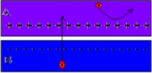
Fig 1: is a diagram that shows the workings of a solar cell's electric field. Note that the section labeled "A" is the n-type junction while the section labeled "B" is the p-type junction. The black arrows in the diagram note the electric field in between the two junctions when external energy is introduced to the system.
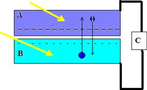
Fig 2: is a diagram that showcases how the current flows in a solar cell as rays of light or photons (the yellow arrows) strike the cell. Again the section labeled "A" is the n-type junction while the section labeled "B" is a p-type junction. The section labeled "C" is the load for the circuit. The electrons will flow starting at point "B" to point "A" then through the load "C." Then the electrons will complete the loop and return in a clockwise loop to point "B."
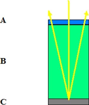
Fig 3: is a diagram of how light (the yellow line) enters the solar cell. It first passes through "A" (the blue region) which is the anti-reflective layer of the cell. The sunlight then travels through, "B," (the green layer) the material the cell is made of, e.g. silicon, gallium arsenide, etc. Then the rays travel the the backing material, "C," (the gray region) which is normally made of aluminum. At this point the photons which remain unabsorbed are reflected off of the backing nd ravel at an angle back out of the cell through both "A" and "B."
Fig 4: is a two dimensional side view diagram that shows the layers to be applied to a solar or photo voltaic cell. "A" is a layer of cover glass to protect the underlying layers. "B" is a layer of anti-reflective layer to prevent photon reflection. "C" is the top contact grid that allows for the transfer of electricity. "D" is the layer of the N-type material. "E" is the layer of P-type material. NOTE: This creates the needed P-N junction. "F" finishes the diagram as the back contact for the conduction of electricity through the cell.
N-Junctions[edit | edit source]
An N-Junction, or negative junction, occurs in a solar cell when the material the cell is made of allows for electrons to break off their respective atom or compound. The newly freed electrons flow over the area causing a generally negative charge.
P-Junctions[edit | edit source]
A P-Junction, or positive junction, occurs when the bonds between the compounds on the panel do not completely fill their valence shells. That is their are "holes" in the valence shell that free flowing electrons can move into. These "holes" move about like their electron counterparts and their positions are determined by the movements of the rest of the electrons moving around the atom or compound.
P-N Junctions[edit | edit source]
When a P-Junction and an N-junction are placed next to each other, a P-N Junction is created and a flow of electric current occurs. The freed electrons from the n-junction side move toward the holes in the p-junction section. This creates the needed electric field to move the electrons to external applications.
Creation of the Gallium Arsenide Crystal[edit | edit source]
There are many ways to create a GaAs solar or photo voltaic cell. First the GaAs crystal must be created. Without this, the solar cell will not be able to function. In this section some methods to create GaAs crystals will be discussed. Three effective means of growing crystals include: Molecular Beam Epitaxy, Metalorganic Vapour Phase Epitaxy, and Electrochemical Deposition (or Electroplating).
Molecular Beam Epitaxy[edit | edit source]
Although this term is rather intimidating when first read, this concept is actually rather simple. In molecular beam epitaxy or MBE a thin film or layer of a given compound is deposited on a heated, crystalline substrate. This is done in a high or ultra high power vacuum. The substrate may be rotated during the process to improve the overall homogenity of the film being created. One of the key reasons MBE is used is it allows for epitaxial growth. This mean that the arrangement of the deposited crystals matches that of the substrate that it is placed upon.
The substrate is placed in an ultra high pressure vacuum. Then the element to be deposited, such as gallium or arsenic, is heated in separate effusion cells. These heated elements are "shot" onto the substrate.
NOTE: The the deposited layer to be of high quality, or pure, care must be taken to ensure that the elements to be evaporated are of high purity and that the process is carried out is a ultra high vacuum.
Metalorganic Vapour Phase Epitaxy[edit | edit source]
Another means of epitaxial growth is metalorganic vapour phase epitaxy. In this process various metalorganic compounds are deposited molecule by molecule into a specific arrangement. Normally this reaction takes place inside of a complex reactor. The reactor, with wall made of stainless steel or quartz, should not reacted with the substrate of the compound to be reacted. The reactor walls generally have a means of cooling down, such as channels for water to flow through. Compounds are normally grown in a hydrogen environment and then form epitaxial layers on the substrate as they decompose.
Electrochemical Deposition[edit | edit source]
When a metallic salt is dissolved in solution, the metal (positive) cation breaks apart from its (negative) anion counterpart. With positive and negative ions in solution, many interesting things can occur when an electric current is routed through said solution. Originally this process was designed to create thin layers of a specific metal. Recently, however, this process has been slightly augmented to create conducting and semi-conducting nanowires. The basic premise behind electrochemical deposition or electroplating, is to negatively charge a substrate and then immerse it in the solution of choice. The negative charge on the electrode (or substrate) attracts the positive metal ions in solution. This causes the metal ions to lie n the surface of the substrate creating a thin layer. This layer usually is about 100 nanometers in thickness; however, the this property can be changed by altering certain factors in the film's creations such as, voltage, solution constituents, temperature and so on.
Other Means of Creation[edit | edit source]
Without one of these means discussed, creating a gallium arsenide solar cell can prove very difficult (especially a high efficiency one). A means is needed to create a this film of gallium arsenide on the respective substrate. It is possible that it can be done by spin coating or very careful application of a gallium arsenide paste or liquid. This may be made by combining gallium arsenide powder and varying quantities of water. These means will most likely not be quite as effective as the others discussed because the order of the gallium arsenide crystal will not be controlled and pristine.
Why Nano Gallium Arsenide Solar Cells?[edit | edit source]
The base function of the GaAs solar cell is to convert the radiant light energy of the sun into electricity. Why use gallium arsenide if other materials that exist can produce a higher efficiency? Well there are a few factors that need to be taken into account. Gallium is even more rare than gold. Cost can be a bit of a detriment. However even in spite of this, gallium arsenide solar cells can produce efficiency levels in the range on 25-30%. This is in the zone that is needed for practical use. Gallium arsenide solar cells can have roughly 25% efficiency rating with only one junction. This makes them a good candidate for a stacked type of solar panels used for collecting light from all across the spectrum.
In a recent article in the magazine Electronic News gallium arsenide was tested on a germanium substrate. The resulting efficiency level was 24.9% for a single junction. This although not amazingly impressive, is high enough to warrant more investigation for full spectrum light capture. The test cell, which was .25 centimeters2, had an open circuit voltage of 999mV, a short circuit current of 29.7 square mA/cm, and a fill factor of 83.2%.
How to make your own gallium arsenide solar cell[edit | edit source]
Although the gallium arsenide solar cell may seem a difficult apparatus to construct. There are distinct steps that can be taken to create one on your own at home or in your lab.
1-Obtain the Substrate[edit | edit source]
Depending what specific properties you want your solar cell to have differing substrates should be used. The most common for use with gallium arsenide are silicon and germanium. These can be fabricated, although these processes were not outlined in this article. They can be purchased in various catalogs and also online.
2-Create the Gallium Arsenide Crystal[edit | edit source]
This is the most difficult step of the solar cell's construction. The gallium and arsenic must be acquired either separately or in the form of gallium arsenide. If the crystal is not created by on of the processes outlined above, the likelihood that it will have high efficiency is very low. The best ways to make a gallium arsenide solar cells were as stated above, molecular beam epitaxy, metalorganic vapour phase epitaxy, and electroplating. To create your gallium arsenide crystal, one of the following must be done:
- Obtain the equipment to allow you to do MBE, MOVPE, or electroplating. This, however as one would imagine, would be rather expensive.
- Build the MBE, MOVPE, or electroplating apparatus. This again would prove fiscally rigorous.
- The cheapest and most probable means to produce a high quality crystal, would be to request access to a lab that has the appropriate equipment to execute the crystal creation.
There are still ways to make a gallium arsenide crystal. Spin coating is one means. This method is very likely to not yield high results. For the spin coating option one would have to acquire a spin coater. This could be a tough task because they are rare and also they can be very expensive. Just like the afore mentioned examples, one should buy, build, or gain access to a spin coater.
Lastly one could create a low quality gallium arsenide crystal by the application of a gallium arsenide paste. This paste can be created by mixing water and gallium arsenide powder in varying amounts. This can then be thinly spread over the substrate. Care should be taken to apply the paste as thinly as possible. NOTE: If using this method, remember that only one layer of gallium arsenide molecules is needed. Thus a thick layer is redundant, unnecessary, and will probably impair efficiency.
3-Creating a Closed Circuit[edit | edit source]
At this point the crystal has been created and is on the appropriate substrate. Now contacts can be placed on the cell at the top and bottom. By creating a closed circuit with the solar or photo voltaic cell as the battery, loads may be placed in the circuit. There should be an anti-reflective layer put on the cell as well as a top glass cover. These serve to increase efficiency and to protect the cell. NOTE: Depending on the efficiency of the cell, size of the cell, and the electrical requirements of the load, the circuit may or may not work.
4-Applying the Sunlight[edit | edit source]
If the solar cell is functional and up to the standards you have set for it by the selection of the load, the application of sunlight should directly power the load on the circuit. Hopefully the solar cell works, the load is working and a new means of renewable energy has been found for the specific load in question.
Future Development[edit | edit source]
Current development has been primarily focused on improving the conversion efficiency of the solar cell. The amount of radiant light converted to actual electricity is the key. Now efficiency levels top out around 30% for our gallium arsenide solar cells. Currently there are a few types of solar cells that can produce a better efficiency rate than that of the gallium arsenide solar cell. Most however top out around 40%. Keep in mind that efficiency levels also vary based on the materials that the solar cell is constructed out of. Below are some of the highlights from the recent past.
- On December 5th 2006 the 40% energy efficiency barrier was broken. With funding from the Department of Energy, Boeing in effort with Spectrolab produced a high end solar cell that had a 40.7% sunlight to electricity conversion rate.
- On July 23, 2007, a group from the University of Delaware using a novel technology that adds multiple innovations to a high-performance crystalline silicon solar cell, achieved a record-breaking combined solar cell efficiency of 42.8 percent from sunlight at standard terrestrial conditions.
Greater Efficiency[edit | edit source]
One type of future development focuses on the development of cells that convert increased levels of the incoming photons to electricity. These would take less incoming energy to begin releasing electrons and would also capture more of their specific wavelength of the light spectrum. There is currently a lot of research on going in this field dealing with making the light rays diffract to increase absorption rates. Normally the rays will reflect of the backing material and travel out of the cell. By creating a lower angle of exit more energy can be absorbed by the cell.
Fig 1: is a diagram of how light (the yellow line) enters the solar cell. It first passes through "A" (the blue region) which is the anti-reflective layer of the cell. The sunlight then travels through, "B," (the green layer) the material the cell is made of, e.g. silicon, gallium arsenide, etc. Then the rays travel the the backing material, "C," (the gray region) which is normally made of aluminum. At this point the photons which remain unabsorbed are reflected off of the backing nd ravel at an angle back out of the cell through both "A" and "B."
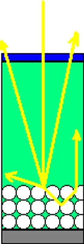
Fig 2: is a diagram showing how better photon (or light rays-the yellow arrows) absorption can be achieved by using materials that diffract (bottom circles) the rays of light so they stay in the material that absorbs the light's energy longer. by creating a lower exit angle (left) the ray's energy stay in the cell longer thus allowing for more absorption. Similarly, if the rays bounce around more (right) the energy is again in the system longer allowing for more time for absorption.
Greater Wavelength Capture[edit | edit source]
The other main area of efficiency development delves into making layered cells that use varying materials for stacked cells. These newly conceived solar cells focus on capturing photons across a wider range of the the spectrum of light. This means that as the light rays pass through these materials their differing wavelengths will be captured by different layers. This can mean that while a normal cell will only take in the energy from a certain range of wavelengths, the accepted range can be increased thereby increasing the efficiency.
Research and Resources[edit | edit source]
These references may be of help in understanding individual parts of this project in greater depth. Due to this I encourage you, the reader, to check out my sources and give me feedback on areas in my article that may need better explanation or further work. Thank You!
Solar[edit | edit source]
- http://en.wikipedia.org/wiki/Solar_cells
- http://en.wikipedia.org/wiki/P-n_junction
- http://science.howstuffworks.com/solar-cell1.htm
- http://science.howstuffworks.com/solar-cell2.htm
- http://science.howstuffworks.com/solar-cell3.htm
- http://www.energy.gov/energysources/solar.htm
- http://www.technologyreview.com/Energy/18415/?a=f
Pearce, Joshua M. "Solar Cells and Photovoltaics." Clarion University of Pennsylvania. Clarion, PA. 2008.
Gallium Arsenide[edit | edit source]
- http://en.wikipedia.org/wiki/Gallium_arsenide
- http://en.wikipedia.org/wiki/Gallium
- http://en.wikipedia.org/wiki/Arsenic
- http://lenntech.com/Periodic-chart-elements/Ga-en.htm
- http://www.lenntech.com/periodic-chart-elements/as-en.htm
Photo Voltaic and Nanotechnology[edit | edit source]
Gallium Arsenide and Solar Cells[edit | edit source]
- http://web.ebscohost.com/ehost/pdf?vid=10&hid=108&sid=aeaf04dc-42b8-4cdb-a6d9-afd068d1d839%40sessionmgr104
- http://web.ebscohost.com/ehost/pdf?vid=6&hid=102&sid=68ca1507-2828-4515-aee0-00222b8793ef%40sessionmgr109
MBE[edit | edit source]
- http://web.archive.org/web/20181024051420/http://www-opto.e-technik.uni-ulm.de:80/forschung/jahresbericht/2002/ar2002_fr.pdf
- http://web.archive.org/web/20070611090826/http://projects.ece.utexas.edu:80/ece/mrc/groups/street_mbe/mbechapter.html
MOVPE[edit | edit source]
- http://en.wikipedia.org/wiki/Metalorganic_vapour_phase_epitaxy
- http://web.archive.org/web/20090703124343/http://www.semiconductor-technology.com:80/glossary/metal-organic-vapour-phase-epitaxy.html


