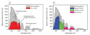
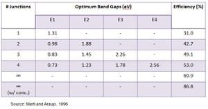
Multi-junction (MJ) solar cells use multiple semiconductorW layers (subcells) to produce electricity at high operating efficiencies. Each layer has a unique band gapW designed to efficiently absorb a specific segment of the solar spectrumW. This has two important advantages over single-junction (SJ) devices: a wider range of absorption of incident photonsW as well as a more effective energy extraction from these photons. The lowest band gap of a MJ cell will be lower than that of a typical SJ band gap. Therefore, the MJ cell can absorb extra photons that possess less energy than the SJ band gap but greater than its own lowest band gap. The MJ cell will absorb the same photons more efficiently since having band gaps closer to the photon energy will reduce thermalization losses. For example, a SJ band gap of 1 eV could extract only 1 eV from a 3 eV photon with 2 eV wasted via thermal decay. On the other hand, a MJ cell with a top band gap of 2 eV will extract twice the energy from the same photon. Figure 1 illustrates the difference in energy absorption between a triple MJ cell and a SJ cell. The colored areas show the amount of energy that can be extracted by each cell. Table 1 gives the optimum band gaps and corresponding efficiencies for MJ cells. The table illustrates how additional junctions raise maximum efficiency. However, adding junctions also increases the device's complexity and cost. It must be noted that the use of concentrators gives an additional boost to potential efficiency.
Power Production[edit | edit source]
Maximizing power generation is the goal of solar cell designing. Power (P) is a simple product of the current (I) and voltage (V) produced:
P = I · V
As a whole, a MJ cell will absorb a greater number of photons and generate more carriers compared to a SJ cell. However, the current produced is in fact lower because each subcell only absorbs photons from a specific segment of the solar spectrum. As the subcells are in series, Kirchoff's lawW dictates that the device's current is limited by the smallest current produced from the subcells (see Current Matching). However, power production of MJ cells is still increased over SJ cells because the drastically higher voltage produced more than makes up for the lower current. Unlike current, the voltage is additive and the multiple band gaps mean a higher voltage is obtained from the incident photons.
Another advantage of a MJ cell is significantly lower resistive losses resulting from its lower current. These power losses (PL) are equal to the square of the current (I) multiplied by resistance (R):
PL = I2· R
This is particularly important for concentrator systems using MJ cells as they produce very high currents.
MJ Cell Structure[edit | edit source]
In a MJ cell, the semiconductor with the highest band gap is used as the top layer. Band gaps are then reduced with each further layer. This design maximizes photon energy extraction as the top layer absorbs the highest energy photons allowing photons with less energy to transmit through. Each subsequent layer then extracts energy from photons closest to its band gap thereby minimizing thermalization losses. The bottom layer then absorbs all remaining photons above its band gap. As Figure 2 shows, cell efficiency is most sensitive to the band gap of the bottom subcell. The error bars indicate the range of subcell band gaps that would maintain a top theoretical efficiency within 1% of ideal. As a result, the material selection for the bottom layer is an extremely important consideration in the design of a MJ device.
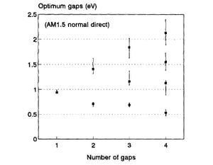
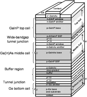
Figure 3 shows the detailed structure of a GaInP (1.8 eV) / GaInAs (1.4 eV) / Ge (0.67 eV) triple-junction solar cell. In this design a wide band gap (transparent) window layer is used to lower a cell's series resistance. It does so by enhancing the lateral flow of photogenerated electrons trying to reach an electrical contact or tunnel junction (see Tunnel Junctions). A buffer layer is also used between the bottom and middle layers to reduce lattice mismatch effects (see Lattice Constant Matching).
Fabrication[edit | edit source]
Multi-junction cells can be constructed mechanically or monolithically. In mechanical stacking, a set of single junction cells with individual sets of contacts and unique band gaps are stacked on top of each other. The bulkiness, cost of additional contacts and substrates and heat dispersing difficulties make this the less favored method. In monolithic cells, each semiconducting layer with its unique band gap is grown sequentially to form a single device with one set of contacts. Metal organic chemical vapour deposition (MOCVDW) is the most common growth procedure used due to its precision, high crystal quality and scalability. Plasma enhanced evaporation deposition is another fabrication method that is easily scalable and highly suitable for semiconductor growth in MJ cells.
Tunnel Junctions[edit | edit source]
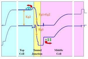
In monolithic cells, the positive and negative contacts are situated on the top and bottom of the cells. As a result, photogenerated carriers produced in the middle semiconductor layers must travel through multiple layers without recombining to reach the contacts. This is one additionally difficulty associated with MJ cells. Tunnel junctions, heavily doped regions connecting the n and p terminals of adjacent layers, are used to aid this carrier transportation. These p-n junctions (typically double hetero junctions) are made with the aim of minimizing electrical losses (voltage drops) as well as optical losses (photon absorption). The latter is done by using wide band gap tunnel junction materials to allow the photons to pass into the lower layers. However, this makes obtaining high tunnelling peak current difficult so thinning the depletion layer by means of a highly doped (>1019 cm -3) junction is necessary. This design promotes quantum tunneling and yet also serves as an effective potential barrier for minority carriers. However, the exact physics behind quantum tunneling are not yet fully understood. Figure 4 on the right shows the band diagram of a double hetero tunnel junction.
Design Considerations[edit | edit source]
Current Matching[edit | edit source]
Since there is only one set of contacts on the top and bottom for a monolithic MJ device, the multiple subcells are connected in series and must obey Kirchoff's current law. This law dictates that current entering and exiting any junction in series must be equal which means a MJ solar cell is limited by the subcell that produced the least current. As a result, current matching for each subcell is of critical importance in the device design. The current produced by each subcell depends on three factors:
- number of incident photons with energy greater than the band gap
- material absorption coefficient
- layer thickness
The number of incident photons can be roughly set by the selection of band gaps for the specific subcell and those above it. The absorption coefficient depends on the specific material. Therefore, the exact matching of subcell currents is performed by adjusting the layer thicknesses. For example, if the number of incident photons reaching each layer are equal, a subcell with a low absorption coefficient must be made thicker in order to absorb the same number of photons (and generate carriers) as the other subcells.
Current matching in MJ cells is extremely important as any difference will result in significant current and efficiency losses. Semiconductors with large absorption coefficients are advantageous to reduce material costs and carrier transportation distances. MJ cells must be carefully designed with respect to band gap selections and layer thicknesses in order to match currents produced by each subcell.
Lattice Constant Matching[edit | edit source]
In monolithic MJ devices, each semiconductor layer is grown on top of one another. However, if the lattice constants of the crystals in adjacent layers do not match this will result in lattice strain and potentially dislocations. These dislocations cause defects to form in the crystal structure leading to unwanted recombinations and subsequently a decrease in cell efficiency. For this reason, it is advantageous to select semiconductor materials that have matching or closely similar lattice constants. Figure 5 shows a list of common MJ semiconductors and their lattice constants. The turquoise lines indicate the lattice constants for mixtures of the two connected materials.
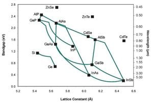
It can be seen that few materials have perfectly aligned lattice constants. For this reason, lattice-mismatched, or metamorphicW, MJ cells are starting to be developed as this allows for a much greater degree of freedom in semiconductor selection. The potential for metamorphic cells lies in the ability of manufacturers to utilize cheaper materials that also possess band gaps near the optimal values for maximum theoretical efficiency. In certain cases, these benefits will outweigh the recombination losses due to lattice mismatch.
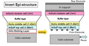
Additionally, there are two main strategies employed to reduce this lattice mismatch effect. The first involves using a buffer layer between two lattice-mismatched materials to match the lattice constants. This buffer layer is typically step-graded meaning its lattice constant is slowly altered by changing the composition so that either end of the buffer layer matches its adjacent subcell. The second method uses an inverted growth method to avoid lattice mismatch effects if the top layers are matched but the bottom layers are not. The growth process is reversed starting with the top layer (widest band gap) and adding subsequent layers. The substrate the top layer was grown on is then etched off after wards. Figure 6 shows the process for a triplet MJ cell for lattice matched top (InGaP) and middle (GaAs) layers with a lattice mismatched bottom cell (InGaAs).
Materials[edit | edit source]
The III-V alloys have proven to be the most suitable semiconductors for MJ devices for a number of reasons. First, the band gaps of the alloys span the spectral range allowing for maximum photon absorption. Second, the alloys have direct band gaps meaning lattice vibrations (phonons) are not required for electron promotion. This avoids the need for additional layer thickness to produce the phonons thereby reducing material costs. Also, the alloys have large absorption coefficients which is another reason only thin layers are needed. The III-V semiconductors can be grown in high volumes with high crystalline and optoelectronic properties making them applicable for large-scale production of commercial solar modules. Finally, the alloys are extremely hard and possess high radiation and temperature resistances so they are ideal for space and extreme weather applications.
InGaN[edit | edit source]
Indium gallium nitride (InGaN) is a III-V alloy with great potential to form cost-effective, ultra high-efficiency MJ solar cells. By varying the indium-gallium ratio in the material its band gap can range from 0.7 eV (InN) to 3.4 eV (GaN) which covers nearly the entire solar spectrum. Since the same three elements are used for different subcells, the large-scale deposition process is simplified with respect to equipment requirements and chamber cleaning. InGaN exhibits nano-columnar growth which increases optical length to enhance light trapping and absorption rates. This columnar structure also reduces strain and defects and increases flexibility and wear resistance on the macro scale.
References[edit | edit source]
Al Naser, Q et al. The Last Development in III-V Multi-Junction Solar Cells. ISECS International Colloqium on Computing, Communication, Control and Management, 2009.
Barnett, A et al. 2007. Milestones towards 50% efficient solar cell modules. 22nd European Photovoltaics Solar Energy Conference
Fetzer, C.M. et al. 2004. High-efficiency metamorphic GaInP/GaInAs/Ge solar cells grown by MOVPE. Journal of Crystal Growth. 261: 341-348
King R.R. et al. 2007. 40% efficient metamorphic GaInP/GaInAs/Ge multijunction solar cells. Applied Physics Letters. 90: 183516
Lee, S.H. et al. 2008. III-IV Multijunction Solar Cells. Iowa State University
Marti, A and Araujo, G. 1996. Limiting efficiencies for photovoltaic energy conversion in multigap systems. Solar Energy Materials and Solar Cells. 43: 203-222
Román, J.M. 2004. State-of-the-art of III-V solar cell fabrication technologies, device designs and applications. Advanced Photovoltaic Cell Design.
Sherif, R.A. et al. The multijunction solar cell: an enabler to lower cost electricity for concentrating photovoltaic systems. Proc. Solar Power Conference 2006.
Takomoto, T. Status of Multijunction Solar Cells and Future Development. CS MANTECH Conference, 2009
Wheeldon J et al. AlGaAs Tunnel Junction For High-Efficiency Multi-Junction Solar Cells: Simulation and Measurement of Temperature-Dependent Operation. Centre for Research in Photonics, U of Ottawa.
Yamaguchi, M et al. 2006. Super high-efficiency multi-junction and concentrator solar cells. Solar Energy Materials and Solar Cells. 90: 18-19, pgs 3068-3077
Yastrebova, N. 2007. High-efficiency multi-junction solar cells: Current status and future potential. Centre for Research in Photonics
- ---
Back to MECH820