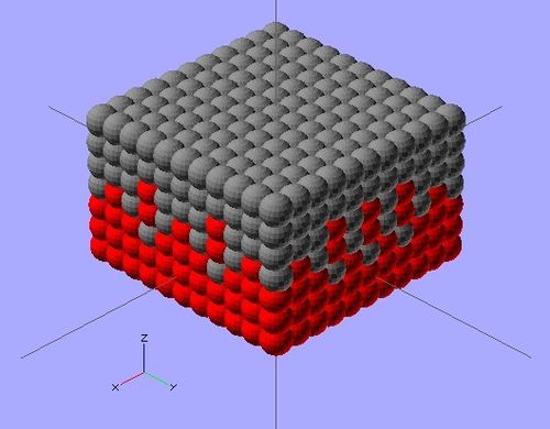
Quantum dots (QD) are nanoparticals comprised of semiconductor materials, which exhibit enhanced electronical properties over bulk materials. These properties are defined by a highly adjustable structure of the quantum dot that yields enormous potential in many applications, including photovoltaic cells.[1] Photovoltaic cells (solar cells) convert light to electrical energy through the use of electron-hole pairs in a circuit. If combined with a quantum dot, a high quantum efficiency (percentage of photons transformed into current) is produced, generating a useable total efficiency.[2] The viability of dissolving these quantum dots into a suitable ink for 3D printing onto a universal solar cell and its processes are analyzed and discussed.
Deliverables
Each project page should contain the following information (All calculations should be transparent and all facts should be cited by appropriate sources and properly wiki referenced
1
- Create your team project page and add the template {{MY3701}}
DONE
2
- A brief description of your semiconductor material with a link to the manufacturer(s) or suppliers of it if it exists on the market.
Needed
3
- A description of how it could be 3D printed (e.g. compare properties like viscosity or melting temperature to existing known printable material)
Our photovoltaic cell would use CdSe and PbS quantum dots to convert photon's energy into current. They will be layered with a n-type (PbS) layer on top, a bulk nanoheterojunction, or mix of the two quantum dot types, in the middle, and a p-type (CdSe) layer on the bottom. There will also be carbon nanotubes dispersed throughout the layers.
The matrix that the quantum dots and single wall carbon nanotubes (SWNT's) would work in is ABS. ABS is already used in many 3D printing applications. It was selected because it has a low enough printing temperature (about 220° C) to work in a low temperature extruder, but a high enough to retain its properties despite extended periods of time in direct sunlight. The ABS that would be used has a resistance of 104 ohm-cm, which would hopefully be improved by the addition of SWNT's.
4
- A detailed BOM of the chemicals used to make it with links to sources and prices in a table - and total cost.
5
- Links to MSDSs for each of the chemicals.
6
- A detailed description of the steps, equipment and amounts of chemicals needed to synthesize the semiconductor ink with references to sources (e.g. recipe)
Ink Synthesis
Sites have been found that would allow us to buy the QD's, ABS, and SWNT's.
The semiconductor will be made using 3 separate inks: a PbS ink, a CdSe ink, and a mixed ink. All of these inks should have 1x10¹⁶ QD's per centimeter3 and 100 mg/L of SWNT's. This process will require a hopper, a heater, a screw extruder, and a mold. The synthesis process of each ink can be summarized with these steps:
- The ABS will be melted at 250° C.
- The melted ABS and appropriate concentrations of QD's and SWNT's will be mixed in a hopper.
- The liquid ink will be extruded in a mold with the same dimension (1.7 mm diameter) as before.
7
- Dia is a program that creates elaborate flowcharts and diagrams to simplify complicated processes. The figures shown to the right outline the basic steps taken to synthesize and 3-D print quantum dots, more specifically CdSe and PbS. The formation of these two quantum dots is also outlined.
8
- Outline purification methods and the methods needed to obtain acceptable purity for your material.
9
- A description of the testing procedures, equipment and specifications for the equipment used to determine if you obtained your target compound.
10
Ideal Semiconductor Ink Properties
This ink is mostly focused on extending the lifetime of charge carriers in the semiconductor. However, another factor that should be considered in the making of this ink, as in all photovoltaic cells, is the range and efficiency of the absorption of photons. These properties will help increase the efficiency of the ink.
- Homogenous distribution of carbon nanotubes among the quantum dots will help conduct improve its ability to act as a charge acceptor.
- Homogenous distribution of the quantum dots allows for more efficient use of the surface area.
- Intermixing of the p-type and n-type QD's in the middle layer to allow a greater interfacial area for diffusion to occur to the junction before recombination occurs within the p- or n-section.
- Range of QD diameters so that a wide range of photon energies can be absorbed.
- Thin layers.
11
In-Situ Analysis
This process takes the trouble of melting and re-solidifying the ABS in a form compatible with the low temperature extruder before 3d printing the ink. This allows us to perform in-situ analysis on the ink before it is printed.
To test the homogeneity of the quantum dots within the ABS, it would be useful to section off some of the semiconductor ink and take an SEM image of the section. A coating of chromium or graphite may need to be applied if the ink is not conductive enough. This in-situ analysis would allow the mixing of the QD's to be tested before they are printed out as a solar cell. Also, if a range of QD sizes are observable within the solidified ink, it follows that a range of photon energies will be able to be observed.
If the ink is not suitably homogenous, the ABS ink can be remelted and remixed, possibly at a higher temperature to increase solubility. This in-situ analysis can be repeated until the ink is suitably homogenous.
12
- List and describe applications of this semiconductor if it is printed.
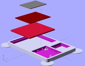
13
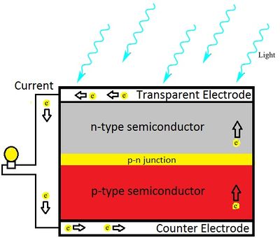
- Make a basic diagram for an electronic device that could use this semiconductor and post diagram in your project page.
A solar cell (also called a photovoltaic cell) is an electrical device that converts the energy of light directly into electricity by the photovoltaic effect. It is a form of photoelectric cell (in that its electrical characteristics—e.g. current, voltage, or resistance—vary when light is incident upon it) which, when exposed to light, can generate and support an electric current without being attached to any external voltage source. [2]
14
- Design the semiconductor portion of the device in OpenSCAD, paste the code directly into your project page
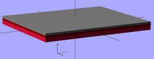
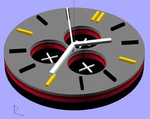
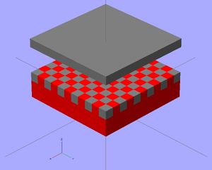
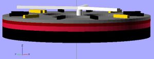
Code for wrist watch:
translate ([0,0,-3.005]) {color ("Black",1) cylinder (h = 3.5, r=25, $fn=100);}
// cutting into the first 2 layers (CdSe)
difference() {
translate ([0,0,.5]) {color ("Crimson",1) cylinder (h = 1.5, r=25, $fn=100);} translate ([0,7,1]) {color ("Crimson",1) circle (6.5, $fn=50); }
translate ([7.25,-5.5,1]) {color ("Crimson",1) circle (6.5, $fn=50); }
translate ([-7.25,-5.5,1]) {color ("Crimson",1) circle (6.5, $fn=50) ; }
}
// cutting into the mixed layer (CdSe + PbS)
difference() {
translate ([0,0,2]) {color ("DarkRed",1) cylinder (h = 1, r=25, $fn=100);} translate ([0,7,1.995]) {color ("DarkRed",1) cylinder (h = 1.5, r=6.7, $fn=50);}
translate ([7.25,-5.5,1.995]) {color ("DarkRed",1) cylinder (h = 1.5, r=6.7, $fn=50);}
translate ([-7.25,-5.5,1.995]) {color ("DarkRed",1) cylinder (h = 1.5, r=6.7, $fn=50);}
}
// cutting into the final layer (PbS)
difference() {
translate ([0,0,3]) {color ("Grey",1) cylinder (h = 1, r=25, $fn=100);} translate ([0,7,2.995]) {color ("Grey",1) cylinder (h = 1.5, r=6.9, $fn=50);}
translate ([7.25,-5.5,2.995]) {color ("Grey",1) cylinder (h = 1.5, r=6.9, $fn=50);}
translate ([-7.25,-5.5,2.995]) {color ("Grey",1) cylinder (h = 1.5, r=6.9, $fn=50);}
}
translate ([1,17,1]) {color ("Gold",1) cube([1,6,4]); }
translate ([-1,17,1]) {color ("Gold",1) cube([1,6,4]); }
translate ([-23,0,1]) {color ("Gold",1) cube([6,1,4]); }
translate ([0,-23,1]) {color ("Gold",1) cube([1,6,4]); }
translate ([17,0,1]) {color ("Gold",1) cube([6,1,4]); }
rotate([0,0,60]) translate ([17,0,1]) {color ("Black",1) cube([6,1,4]); }
rotate([0,0,30]) translate ([17,0,1]) {color ("Black",1) cube([6,1,4]); }
rotate([0,0,120]) translate ([17,0,1]) {color ("Black",1) cube([6,1,4]); }
rotate([0,0,150]) translate ([17,0,1]) {color ("Black",1) cube([6,1,4]); }
rotate([0,0,210]) translate ([17,0,1]) {color ("Black",1) cube([6,1,4]); }
rotate([0,0,240]) translate ([17,0,1]) {color ("Black",1) cube([6,1,4]); }
rotate([0,0,300]) translate ([17,0,1]) {color ("Black",1) cube([6,1,4]); }
rotate([0,0,330]) translate ([17,0,1]) {color ("Black",1) cube([6,1,4]); }
translate ([0,-1.5,0]) {color ("White",1) cylinder (h = 6, r=1, $fn=50);}
rotate([0,0,35]) translate ([-1,-2,6]) {color ("White",1) cube([14,1.5,1]); }
rotate([0,0,270]) translate ([1,-.5,6]) {color ("White",1) cube([18,1.5,1]); }
rotate([0,0,120]) translate ([-1,.5,6]) {color ("White",1) cube([22,.5,1]); }
// small circles
rotate([0,0,0]) translate ([0,4,1]) {color ("White",1) cube([.5,6,.5]); }
rotate([0,0,0]) translate ([-2.75,6.75,1]) {color ("White",1) cube([6,.5,.5]); }
rotate([0,0,235]) translate ([-.25,6,1]) {color ("White",1) cube([.5,6,.5]); }
rotate([0,0,235]) translate ([-2.75,8.75,1]) {color ("White",1) cube([6,.5,.5]); }
rotate([0,0,135]) translate ([.5,6,1]) {color ("White",1) cube([.5,6,.5]); }
rotate([0,0,135]) translate ([-2.25,8.75,1]) {color ("White",1) cube([6,.5,.5]); }
15
http://www.appropedia.org/File:Watch_Face_STL.stl
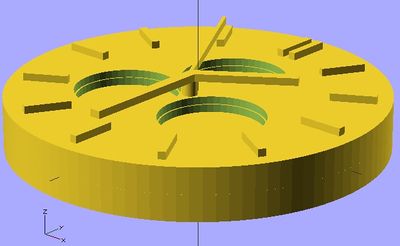
To make bullets use the asterisk:
- Like this
- and like this
- and two for the next indent
- and back to one...
Important Facts about quantum dots
- to generate more than one electron-hole pair for every photon absorbed.[3]
Project goals
To make a numbered list use the pound sign:
- Like this
- and like this
- See Help:Contents for more formatting code.
Design
Describe your design here.
- Sample gallery
-
More sample caption text. This would look better with different images. :)
-
Even more sample caption text.
Next level heading
You may need deeper level headings. Just keep adding equal signs to get that.
Costs
You may describe your costs here.
| header 1 | header 2 | header 3 |
|---|---|---|
| row 1, cell 1 | row 1, cell 2 | row 1, cell 3 |
| row 2, cell 1 | row 2, cell 2 | row 2, cell 3 |
See Help:Tables and Help:Table examples for more.
Discussion
Your discussion.
Next steps
The next steps.
Conclusions
Your conclusions.
References
- ↑ Solarcellcentral October 11, 2013.
- ↑ [Solar Cell - Wikipedia] October 11, 2013.
- ↑ Solarcellcentral October 11, 2013.
Contact details
Add your contact information.
