The purpose of this page is to outline the process of 3D-printing organic semiconductors to prototype a photovoltaic sticker that can be adhered and that will supply power to a number of electronic devices. The photovoltaic effect, organic semiconductor properties & synthesization , and 3D-printing of the solar cell will be outlined. Furthermore, an OpenSCAD model for the rapid prototyping of the product will be introduced and the applications explained.
Photovoltaic Cells
Photovoltaic Effect
- The photovoltaic effect is a response between two different materials to radiation. When the materials are irradiated, the response creates a potential difference where the materials meet. This charge can be collected and used to power electronic devices.
- Solar cells consist of an absorber layer with semi-permeable membranes on either side of the absorber, typically an n-type semiconductor. The n-type semiconductor has a large electron conductivity due to proportionally large differences in electron and hole concentration. In contrast, p-type semiconductors have a large hole conductivity due to the amount of electrons generated when light is absorbed. The asymmetry in the structures of these semiconductors is the basis for the photovoltaic effect.
- The efficiency of the solar cell is limited by the mobility of electrons and holes generated during absorption. It is important to limit the thickness of the absorber so that the charge carriers will reach the hole membrane. If the thickness of the absorber is larger than the diffusion capabilities of the charge carriers, no electric field will be generated.
Organic Semiconductors
- Organic semiconductors in photovoltaic cells exhibit many advantages to crystalline silicon (c-Si) and other inorganic semiconductors. The use of organic semiconductors is becoming a competitive option in the photovolatic industry because they can be used with flexible substrates, are low in cost production,and exhibit characteristics that make them environmentally stable 41.
Bilayer Photovoltaic Cell
- A bilayer PV cell consists of a cathode, buffer layer, active layer, and anode 41. In an organic photovoltaic cell, a photon is absorbed through the cathode and buffer layer into the the active layer where then an exciton -electron-hole pair- is formed. The purpose of the buffer layer is to improve charge transportation; it is an added transition area. The active layer consists of a donor and acceptor semiconductor. The excition will travel through the donor layer and at the donor-acceptor interface the exciton will separate into an electron and hole. The electron travels through the acceptor and the hole will travel back through the donor. From here the acceptor penetrates the anode, performing electrical work. The thicker the buffer layer, the more likely the exciton will recombine before reaching the donor-acceptor interface. Recombination of an electron-hole pair dooms its ability to do electrical work. The layer must be thick enough to absorb most of the light, yet thin enough to minimize recombination loss. The difference in bandgap for each semiconductor is important, and must be optimized to maximize the portion of the solar spectrum that the PV cell can capture. 32.
Photovoltaic Material
- The materials used are specific to their function in the PV cell. The cathode and anode layer must be conductors and have differing work functions. The front electrode must have a lower work function than the back electrode in order to collect holes. The materials chosen were ITO, Indium Tin Oxide, for the cathode and Al, Aluminum, for the anode. The buffer layer is a PEDOT-PSS, poly(3,4-ethylenedioxythiophene) poly(strenesulfonate), a conductive polymer. It acts as a buffer between the mismatched energy levels of the cathode and active layer. The active layer consists of a donor layer and acceptor layer. The donor layer is a P3HT, poly(3-hexylthiophene-2,5-diyl). The acceptor layer is a PCBM, phenyl-C61-butyric acid methyl ester. The P3HT and PCBM interface will generate an internal electrical potential that can be captured by the electrodes. The potential energy is converted to electrical energy which can be used to power a device. PVC, polyvinyl chloride, will be used as the thin-layer substrate due to its unique capability to form a temporary electrostatic bond to electronic devices to eliminate the need for an adhesive.
- Exciton diffusion length and work function are important factors in determining the materials and thickness of materials used. The exciton diffusion length directly correlates to the thickness of the material. Organic materials are estimated to have a diffusion length of approximately 5-20 nm. The equation

- describes the distance the exciton can travel before recombination 32. Through the use of this equation it was estimated that each layer of organic semiconductor must have a minimum thickness of 10 nm, while the anode and cathode must have a minimum thickness of 5 nm. The equation

- illustrates the energy needed to remove an electron from the surface of the electrodes, anode and cathode 32. The work functions required for the anode and cathode are specific in order to remove electrons and collect holes. The cathode must have a lower work function then the anode.


- Figure 1
- This solar cell will be 3D-printed using three organic inks: PEDOT:PSS ,P3HT, PCBM.
3D-Printing
Description
- Fused filament fabrication will be used to create a 3-dimensional object through the use of a standard data interface program, STL 3334. This device, designed in OpenSCAD, can be 3D-printed. The synthesized organic semiconductors are heated in a vacuum and layered onto a substrate in the order indicated in the code. This method is beneficial in that layer thickness can be easily adjusted and an unlimited amount of materials can be layered.
- The synthesized organic semiconductors will be layered on the Al substrate in a determined order. The sequential order will be PCBM, P3HT, and PEDOT-PSS. A final metal of ITO is to be layered on the top of PEDOT-PSS, however the largely differing melting points creates a difficulty in 3D printing a metal on a polymer. Current 3D printers do not have this capability, future advancements to the technology are necessary. Alternatively, the Al and ITO could be purchased and added to the PV cell after the printing of the organic semiconductors.
- The final step of printing the organic PV sticker is to rotate the PV cell 180 degress so that the Al substrate is facing up. A thin layer of polyvinyl chloride will be 3D-printed on the surface of the Al. This is done to provide a non-destructive adhesive layer for the PV sticker.
Advantages of 3D-Printing
- Rapid prototyping
- speeds time to market
- Reduce traditional processing costs
- cuts prototyping and tooling costs
- eliminates design errors faster
- Printing cycle repetition
- limits processing inconsistencies
- Cheap manufacturing
- Complexity
- complex objects are more easily 3D printed than machined
- cuts material waste
- Customization
- product can be customized, printed with alternative materials, etc.
Table 1: Bill of Materials
| No. | Material | Price | Units Needed | Cost of Material |
|---|---|---|---|---|
| 1 | PEDOT:PSS | $139.00/250g9 | 100 g | $55.60 |
| 2 | P3HT | $175.00/250g11 | 100 g | $70 |
| 3 | PCBM | $829.00/100mg8 | 1g | $8.29 |
| 4 | PVC | $44.00/500g10 | 100g | $8.80 |
| 5 | Indium Tin Oxide | $298.00/100g7 | 1 ft × 1 ft × 5 mm | $23.70 |
| 6 | Aluminum | $0.66/g5 | 100g | $6.60 |
| 7 | Chlorobenzene | $99.50/L6 | 1L | $99.50 |
| Total Cost | 272.50 | |||
Refer to Figure 1
- All materials to be purchased from Sigma-Aldrich Co.
- Material to manufacture 100 cells
Synthesize Semiconductor Ink
- The materials needed to synthesize the polymers for this project can be purchased from the company Sigma Aldrich. To comply with the understanding of the production and process of synthesization, it is necessary to look at synthesizing each layer of the semiconductor. The ink used to produce the 3D image must be synthesized from the original material. When undergoing the process of synthesis, the organic polymer's layers must be accounted for. Referring to Figure 1, the pictorial illustrates layers of the Organic Photovoltaic Sticker. The anode and cathode casing is made up of Indium Tin Oxide and Aluminum, respectively. The intermediate layer seen is made up of PCBM, the acceptor layer, and P3HT, the donor layer. This is called the active layer. The buffer layer consists of PEDOT-PSS which resides between the anode and active layer.

- Figure 2
- The process to synthesize an organic semiconductor involves the addition of Cholorbenzene (C6H5Cl)42. P3HT and PCBM must be dissolved in equivalent amounts with C6H5Cl; the suggested ratio is 1:1. The production of this concentration is estimated to require a solution of 20-60 mg/mL. Sterile substrates are used to allow synthesis of up to six cells per slide. The final desired surface area for the device is 1 cm by 1 cm. Each layer must be stirred and then left to cool before proceeding to the additional layer. The buffer material, PEDOT:PSS, used is spin coated in order to ensure it is deposited to the substrate. This process uses centrifugal force and must be done at a high speed in order to achieve the anticipated thickness. The PEDOT layer must then be annealed after excess is removed from the substrate. Annealing must be done at a maximum of 120°C. The P3HT and PCBM solution is filtered again and small amounts are deposited to each ITO slide. A minimum of 0.5 mL is required. A similar process to the spin coating of the PEDOT layer is replicated with the solution. The excess active solution must be removed before the ITO slide is annealed. The proposed temperature should not exceed 150°C. The process of annealing the solution forces an aluminum electrode to evaporate from the substrate. The final substrate is now complete with six synthesized solar cells in a processable ink for and is ready to be 3D printed 41.
- The PVC must also be synthesized in order to produce an ink that can be printed on the surface of the anode layer of the semiconductor. This self-adhesive film is purchased in liquid form and could be applied after the photovoltaic cell is 3D-printed.
Purification
- It is necessary to ensure that purified materials are used as components in the procedure and production of the ink. Acceptable purity standards are derived from the synthesis of the layers of each material within the organic semiconductor. Cholorbenzene requires a purity of 99%. Chemicals used in cleaning and sterilizing the equipment and substrates should have a minimum purity of 99.5% pure. Polyvinyl chloride is a thermo-plastic organic polymer that has additive features that ensure flexibility. Plasticizers are used within the material to improve overall durability and flexibility. Di-n-butyl phthalate is soluble within the polymer and allows the characteristics of a flexible and soft material to be achieved in our supply of polyvinyl chloride38. Therefore, it is only necessary to purchase 99%> pure PVC if there are intentions to use diverse plasticizers or to independently embed alternate plasticizers.
Best In Class Materials
Table 2: Properties of Semiconductor Materials
| Ink Material | Young's Modulus | Electrical Conductivity | Power Conversion Efficiency | Melting Point | Band Gap | Features | MSDS |
|---|---|---|---|---|---|---|---|
| PEDOT:PSS | 2.00 GPa48 | 26.1 S cm-114 | 3.72%37 | 146 °C14 | 1.5-1.6 eV3 | anti-static, anti-reflective15 | PEDOT:PSS 29 |
| P3HT | 0.22 GPa49 | 2.30(10-5) S cm-113 | 3.60%36 | 233 °C21 | 1.9-2.0 eV4 | donor material19 | P3HT 31 |
| PCBM | 3.06 GPa47 | 2.70(10-3) S cm-1 12 | 4.40%35 | 290 °C20 | 1.3-1.9 eV[1] | high electron conductivity, low hole conductivity18 | PCBM 28 |
Table 3: Properties of Other Materials Used
| Material | Young's Modulus | Melting Temperature | Use | Features | MSDS |
|---|---|---|---|---|---|
| PVC | 3.0-3.3 GPa39 | 80 °C39 | Creates static cling on the outside of a phone so the sticker can adhere to the surface without the damage of using a permanent adhesive40 | lasts greater than 100 years, high thermal power, eco-efficient,recyclable, economical40 | PVC |
| Indium Tin Oxide | 116 GPa46 | 1900 °C24 | Used as a cathode casing43 | high optical transmittance, low electrical resistivity, wide electrochemical window43 | ITO |
| Aluminum | 69.0 GPa45 | 660 °C22 | Anode Casing44 | absorbs anodized surfaces, light weight, reflects electromagnetic waves16 | Aluminum |
| Chlorobenzene | N/A | -46 °C23 | Used to make a soultion with P3HT | colorless, neutral liquid17 | Chlorobenzene |
Characterization
- The technique best fit for the characterization of the chemical composition of this product is scanning auger microprobe spectroscopy (SAM). SAM has an impressive maximum z-resolution of 0.5 nm and is particularly useful for analyzing thin films. The instrument is a combination of SEM and Auger electron spectroscopy (AES). AES is very sensitive to light elements compared to other surface characterization techniques. This is mainly due to the fact that production of Auger electrons is dominant over characteristic X-ray production for elements with an atomic number less than Si. This high sensitivity is ideal for characterization of an organic PV cell. Auger electrons have a characteristic energy level that can be quantified and linked to a particular element, a sort of electrical tag. Another advantage to this technique is the ability to ion mill. Ion milling is the bombardment with inert ions to sputter away layers of atoms on the material surface and can be done in-situ 2. By sputtering away layers of atoms over an area , the layers of PEDOT:PSS, P3HT, and PCBM semiconductors used for this PV cell can be characterized with relative ease.
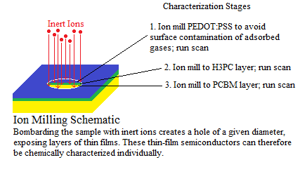
- Figure 3

- Using ion milling, the chemical purity of the inks can be accurately analyzed post-production. It will also provide structural information as well since the SEM is visually helpful. SAM has the ability for point, line, or area scans. For this application, an area scan will be used since we are interested in the chemical purity of the individual inks.
- The analysis will proceed as follows:
- The purchased or synthesized materials will be scanned individually to determine chemical purity before conversion into ink.
- The solar cell will be milled to eliminate any residual gases that may have adsorbed on the surface.
- The first area scan will be run on the milled area to determine chemical purity of PEDOT:PSS ink.
- The specimen will again be carefully sputtered to the P3HT absorber layer.
- A second area scan will be conducted to determine the chemical purity of the P3HT ink.
- The specimen will be carefully milled to expose the PCBM layer.
- A final area scan will be conducted to determine the chemical purity of the PCBM ink.
- Since SAM and our selected 3D-printing technique operate under ultra-high vacuum conditions, the semiconductor layers can also be profiled individually during printing, which can help reduce material waste by ion milling.
- It is also important to characterize the electrical potential of the device to determine information regarding total power output capability, energy conversion efficiency, and the output voltage and current. The technique best fit for the characterization of these properties is Electrochemical Capacitance-Voltage profiling (ECV). Capacitance is measured as a function of voltage in this technique and yields an output graph of voltage vs. capacitance. From these graphs, one can determine layer thickness, charges, average concentration of adsorbed contaminants and trapping density. Additionally, this technique can be adapted for in-situ analysis during ink synthesis and during printing. The ink could be synthesized on a thin metal substrate and a small low-density metal could be floated in the ink. The leads of the instrument could then be attached to the anode and cathode for in-situ ECV profiling. For this technique to be used during the printing process, the process would be paused for measurement as the individual semiconductor layers are printed. Though this method would be relatively slow, it could potentially provide information that would prevent further material waste. Additionally, this process could be used for setting purification standards. 50 Why ECV?.
- Additional Characterization Techniques to Consider
- XRD, XREDS
- Chemical composition
- RBS
- Chemical composition
- Resistivity profiling
- Electrochemical information
- Hall Effect profiling
- Efficiences
- Additional Characterization Techniques to Consider
Applications
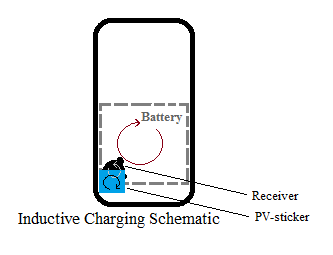
- These photovoltaic stickers were designed to be applied to small electronic devices like phones, tablets, laptops, cameras, etc. Though an external circuit was not part of the design process, devices that already use inductive charging technology will be able to capture power from this product. Inductive charging is a wireless method of charging or powering a device. An example of such a device is the new Samsung Galaxy S4 by Android. A receiver, or signal converter, has been fixed to the battery. This receiver is necessary for the inductive charging of the device and, without it, the inductive current released by the charging station would simply be dissipated. For example, if one tried to charge an iPhone5 on the same charging station, the iPhone would be incapable of accepting power from the device due to the lack of a receiver to convert the inductive current into power. These 3D-printed solar cells will become increasingly useful as inductively coupled charging technology advances are improved and as more consumer electronics companies begin to implement this technology. They primary drive coil, in this case the PV sticker, that can be harnessed by a receiver directly attached to a battery. Moreover, these solar cells are not a standalone product but require further development in inductive charging technology or an external circuit for use 51.
- Figure 4

- For inductive charging to occur, a primary drive coil must induce a current on the secondary coil, the receiver. The receiver will then power the device by inducing a current on the battery. If the device already has a secondary coil then the photovoltaic sticker could simply be applied near this secondary coil to charge the device.
- Inductive charging is an inefficient process now (approximately 3-6.5% power conversion 51) but efficiency can be expected to become improve as technological development moves forward. Overall, this charging method is safer and more convenient than conventional charging methods. The electronics of the target device will also be better protected since there will be no need for external cavities for wire terminals. Additionally, combining inductive charging and solar cell technology would be a large step for green energy; this device would be environmentally friendly and could be easily replicated and rapidly prototyped,eliminating the need for charging cords and unnecessary power waste.
Design
- The following schematics were generated using OpenSCAD software 33 OpenSCAD User Manual and represents the model for our photovoltaic cell.
- The .stl file can be found here File:STLCELL.stl
 Top View
- Figure 5
 Side View
- Figure 6
 Orthorhombic Perspective
- Figure 7
 Sandwich View
- Figure 8
- The dimensions of the cell are 1 cm x 1 cm x 70 nm
- This is the code for the rapid prototyping of our organic PV stickers.
module PVCELL()
//Scale: 10E-8 m
//Cathode Contact (GRAY)
translate([0,0,-5.5])
color([1,1,1]) cube([100000,100000,0.5],center=true);
//PEDOT:PSS WINDOW (BLUE)
translate([0,0,-1]) color([0,0,1]) cube([100000,100000,1],center=true);
//H3PT ABSORBER (GREEN)
translate([0,0,-2]) color([0,1,0]) cube([1000,1000,1],center=true);
//PCBM ACCEPTOR (YELLOW)
translate([0,0,-4]) color([255,255,0]) cube([100000,100000,3],center=true);
//Anode Contact (GRAY)
color([1,1,1]) cube([100000,5,0.5],center=true);
color([1,1,1]) cube([5,100000,0.5],center=true);
translate([100,0,0]) union(){ color([1,1,1]) cube([5,100000,0.5],center=true);}
translate([200,0,0]) union(){ color([1,1,1]) cube([5,100000,0.5],center=true);}
translate([300,0,0]) union(){ color([1,1,1]) cube([5,100000,0.5],center=true);}
translate([400,0,0]) union(){ color([1,1,1]) cube([5,100000,0.5],center=true);}
translate([500,0,0]) union(){ color([1,1,1]) cube([5,100000,0.5],center=true);}
translate([-100,0,0]) union(){ color([1,1,1]) cube([5,100000,0.5],center=true);}
translate([-200,0,0]) union(){ color([1,1,1]) cube([5,100000,0.5],center=true);}
translate([-300,0,0]) union(){ color([1,1,1]) cube([5,100000,0.5],center=true);}
translate([-400,0,0]) union(){ color([1,1,1]) cube([5,100000,0.5],center=true);}
translate([-500,0,0]) union(){ color([1,1,1]) cube([5,100000,0.5],center=true);}
translate([0,499,0]) union(){ color([1,1,1]) cube([100000,5,0.5],center=true);}
translate([0,-499,0]) union(){ color([1,1,1]) cube([100000,5,0.5],center=true);}
translate([0,250,0]) union(){ color([1,1,1]) cube([100000,5,0.5],center=true);}
translate([0,-250,0]) union(){ color([1,1,1]) cube([100000,5,0.5],center=true);}
//Rotate for printing PVC on bottom of cathode
rotate(180,[0,1,0]);
//PVC (RED)
translate([0,0,-6.5]) color([1,0,0]) cube([100000,100000,1],center=true);
PVCELL();
Group Members & Contact
- Laura Jewett
- User:Lmjewett
- Sukaina Miftah
- User:Samiftah
- Alexander Reinl
- User:Adreinl
- Annie LeSage
- User:Aelesage
References
1 Additive 3D-printing in Industry
2 AES Mechanics
3 Band Gap PEDOT:PSS
4 Band Gap P3HT
5 Cost of Aluminum
6 Cost of Chlorobenzene
7 Cost of ITO
8 Cost of PCBM
9 Cost of PEDOT:PSS
10 Cost of PVC
11 Cost of P3HT
12 Electrical Conductivity PCBM
13 Electrical Conductivity P3HT
14 Electrical Conductivity & Melting Point of PEDOT:PSS
15 Electrical & Thermal Properties of PEDOT:PSS
16 Features of Aluminum
17 Features of Chlorobenzene
18 Features PCBM
19 Features P3HT
20 Melting Point PCBM
21 Melting Point P3HT
22 Melting Temperature Aluminum
23 Melting Temperature Chlorobenzene
24 Melting Temperature ITO
25 MSDS for Al
26 MSDS for Chlorobenzene
27 MSDS for InSnO
28 MSDS for PCBM
29 MSDS for PEDOT:PSS
30 MSDS for PVC
31 MSDS for P3HT
32 Numerical Simulation of Organic PV Cells
33 OpenSCAD User Manual
34 Organic Semiconductors in Electronics
35 Power Conversion Efficiency PCBM
36 Power Conversion Factor P3HT
37 Power Optimization of PEDOT:PSS
38 Purification of Organic Solids
39 PVC Properties
40 PVC Usage/Features
41 P3HT:PCBM Synthesis
42 Spin Coating of Low Bandgap Polymers
43 Usage/Features of ITO
44 Use Aluminum
45 Young's Modulus Aluminum
46 Young's Modulus ITO
47 Young's Modulus PCBM
48 Young's Modulus of PEDOT:PSS
49 Young's Modulus P3HT
50 Why ECV?
51 Wireless Power Transfer