| Line 17: | Line 17: | ||
===Copper Indium Gallium Selenide (CIGS) and there application in Photovoltaic Cells=== | ===Copper Indium Gallium Selenide (CIGS) and there application in Photovoltaic Cells=== | ||
[[Photovoltaics]] are devices which convert light energy into electrical energy. Photovoltaic (PV) cells can generate electricity for a wide range of electrical applications | [[Photovoltaics]] are devices which convert light energy into electrical energy. Photovoltaic (PV) cells can generate electricity for a wide range of electrical applications and can be implimented in most geographical locations and theoretically at any scale. A PV cell is only as good as the semi-conductor materials for which it is composed of. Specifically in this page we will be discussing [[copper indium gallium selenide]] as a semi-conductor material in a PV cell. Aside from just PV cells, according to the National Centre for Photovoltaic Research and Education (NCPRE), there are criteria we must evaluate of a semi-conductor material before we implement it in a design. | ||
*Absorption Coefficient: | Those include: | ||
*Abundance of Raw materials: The materials used | |||
*Toxicity of material: The material must be non | *Absorption Coefficient: The higher the absorption coefficient the thinner the semi-conductor material can be. For thin film applications, this trait is preferred. | ||
*Stability of the material & junction: The material must be stable | *Abundance of Raw materials: The semi-conductor materials used in any application must be readily available at a reasonable cost. | ||
*Radiation resistance: | *Toxicity of material: The semi-conductor material must be non-hazardous to the environment. | ||
*Stability of the material & junction: The chosen material for an application must be able to withstand the climate it is placed in and be chemically stable. | |||
*Radiation resistance: Specifically speaking in most photovoltaic applications the semi-conductor material must not degrade to high energy radiation it may be exposed to. | |||
To speak specifically about Copper Indium Gallium Selenide (CIGS) as an absorbing layer in PV cells we can note that: | To speak specifically about Copper Indium Gallium Selenide (CIGS) as an absorbing layer in PV cells we can note that: | ||
Copper Indium Gallium Selenide in its chemical form is expressed as Cu(In,Ga)Se2, which belongs to the family of I-III-VI2 semiconducting materials that crystallize in a tetragonal chalcopyrite structure. Due to the high absorption coefficient and a direct band gap of 10^5/cm, 1.04 eV - 1.70 eV respectively a very think layer of CIGS is required perform the actions require in a PV cell. CIGS are also unique in that varying the Ga percentage the band gap can be tailored to be optimized in any situation. Specifically speaking we can tailor the band gap from 1.04 eV to 1.7 eV by changing the percent Ga. This unique ability of CIGS makes it an excellent material to be used in indoor applications (calculators etc.) along with large scale applications (solar fields, terrestrial etc...) | |||
'''EDITED TO THIS POINT DON'T CHANGE ABOVE FOR NOW.''' | |||
CIGS based solar cells are constructed in two possible models; a Substrate Model or a Superstrate Model. See Figure 1 for more details. | CIGS based solar cells are constructed in two possible models; a Substrate Model or a Superstrate Model. See Figure 1 for more details. | ||
Revision as of 22:01, 24 September 2012

|
This page was part of a project for MY3701 -- an MTU class on semiconductors.
Do NOT edit this page -- please only leave comments using the discussion tab. |
Project Description
As taken from the MY3701 Semiconductor recycling project page: Pure semiconductors are extremely valuable materials, but due to the relative youth of the industry (as compared to metals), semiconductor recycling has not been fully utilized. Your project is to design a semiconductor materials recycling plant to support a product of your choice that contains one or more semiconductors and determine its technical viability.
Deliverables
Copper Indium Gallium Selenide (CIGS) and there application in Photovoltaic Cells
Photovoltaics are devices which convert light energy into electrical energy. Photovoltaic (PV) cells can generate electricity for a wide range of electrical applications and can be implimented in most geographical locations and theoretically at any scale. A PV cell is only as good as the semi-conductor materials for which it is composed of. Specifically in this page we will be discussing copper indium gallium selenide as a semi-conductor material in a PV cell. Aside from just PV cells, according to the National Centre for Photovoltaic Research and Education (NCPRE), there are criteria we must evaluate of a semi-conductor material before we implement it in a design. Those include:
- Absorption Coefficient: The higher the absorption coefficient the thinner the semi-conductor material can be. For thin film applications, this trait is preferred.
- Abundance of Raw materials: The semi-conductor materials used in any application must be readily available at a reasonable cost.
- Toxicity of material: The semi-conductor material must be non-hazardous to the environment.
- Stability of the material & junction: The chosen material for an application must be able to withstand the climate it is placed in and be chemically stable.
- Radiation resistance: Specifically speaking in most photovoltaic applications the semi-conductor material must not degrade to high energy radiation it may be exposed to.
To speak specifically about Copper Indium Gallium Selenide (CIGS) as an absorbing layer in PV cells we can note that:
Copper Indium Gallium Selenide in its chemical form is expressed as Cu(In,Ga)Se2, which belongs to the family of I-III-VI2 semiconducting materials that crystallize in a tetragonal chalcopyrite structure. Due to the high absorption coefficient and a direct band gap of 10^5/cm, 1.04 eV - 1.70 eV respectively a very think layer of CIGS is required perform the actions require in a PV cell. CIGS are also unique in that varying the Ga percentage the band gap can be tailored to be optimized in any situation. Specifically speaking we can tailor the band gap from 1.04 eV to 1.7 eV by changing the percent Ga. This unique ability of CIGS makes it an excellent material to be used in indoor applications (calculators etc.) along with large scale applications (solar fields, terrestrial etc...)
EDITED TO THIS POINT DON'T CHANGE ABOVE FOR NOW.
CIGS based solar cells are constructed in two possible models; a Substrate Model or a Superstrate Model. See Figure 1 for more details.
- Substrate Model: The back contact lies on a glass substrate, and light falls on solar cell top layer. For this extra passivation is required to avoid degradation of the solar cell.
- Superstrate Model:the front contact lies on a glass substrate and light falls from top of the surface. The benefit of this is it does not require any extra passivation.

The construction of CIGS as the majority absorbing layer can be done multiple ways, including:
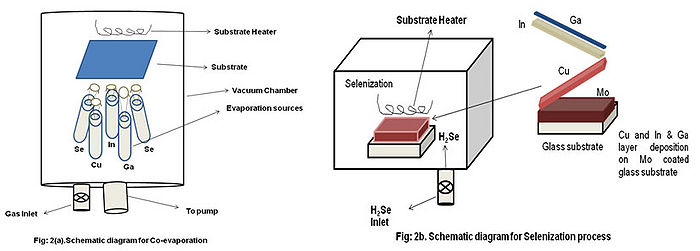
- Co-Evaporation
- Here a three stage process is used.
- 1st stage:- Deposition of In ,Ga and Se at relatively low temperature,
- 2nd stage:- Cu rich growth stage by evaporating Cu in excess at elevated temperature
- 3rd stage:- Deposits only In, Ga and Se to ensure the overall Indium (In) rich composition of the film.
- Co-evaporation method requires high substrate temperature more than 450-500 oC to get CIGS phase.
- Selenization
- In this method, first of all stacked layers of Cu, In and Ga are deposited on the Mo coated glass substrate. Then selenization takes place under H2Se. To improve the device **performance, a second thermal process under H2Se is added, resulting in an absorber that is Cu(In,Ga)(S,Se)2 rather than Cu(In,Ga)Se2 . The problem with this method is that, H2Se **is very toxic, requiring great precaution. This method also requires high substrate temperature to get the CIGS phase.
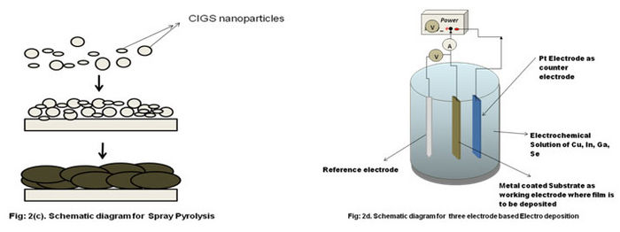
- Spray Pyrolysis
- In spray pyrolysis, CIGS colloidal / precursor solutions are prepared mostly by CuCl2, InCl3, SC(NH2)2 , and GaCl3. Precursor films are then sprayed onto a preheated glass **substrate at a constant temp of 350-400 oC. Post deposition annealing is performed in various environments such as H2, H2Se etc at 450-500 oC.Solar efficiency reached with spray **pyrolysised absorber is low compared to other methods.
- Electrodeposition
- In this method electrochemical solution containing Cu, In, Se, Ga in appropriate amount is used. According to the Nernst equation, the electrode potential for selenium and copper **being more positive than that for indium, deposition of selenium and copper is expected to precede the indium deposition. For simultaneous deposition of Cu, In, Ga and Se, the **concentration and pH of the electrolyte should be adjusted such that the electrode potentials of all the individual deposits may come closer to each other. A relatively higher **concentration of indium shifts its potential in the positive direction approaching closer to that of Cu and Se. The presence of Cu in the electrolyte solution enhances the **deposition of Se with Cu. It shows a three-electrode setup which is used commonly in electrodeposition. Two of the electrodes, the working electrode and the counter electrode, **are connected to the power source. The substrate is connected as the working electrode, and an inert electrode, often a Pt wire or plate, is used as the counter electrode. The **third electrode, that is, the reference electrode, is needed in potentiostatic electrodeposition where the potential of the working electrode is controlled in a predetermined **way. The potentiostat measures and controls the potential of the working electrode with respect to the reference electrode. Note that the potential of the reference electrode **must be known, and furthermore it must stay constant during the deposition. To satisfy the latter requirement, no current is allowed to flow through the reference electrode. **Silver-silver chloride electrode (Ag/AgCl) and calomel electrode (Hg/Hg2Cl2) are commonly used reference electrodes.
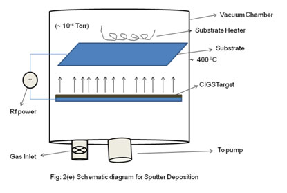
- Sputtering
- In sputtering, CIGS target may be used to deposit CIGS thin films.
See Figure 2, 3 and 4 below for construction diagrams for all process's described above.


Companies currently producing copper indium gallium selenide (CIGS) photovoltaic cells include:
- Ascent Solar Technologies
- DayStar Technologies
- Global Solar Energy
- HelioVolt
- Honda Soltec
- International Solar Electric Technology
- IBM
- ICP
- Miasole
- Nanosolar (printed electronics)
- Odersun
- Q-Cells-Solibro
- Solar Frontier (formerly a division of Showa Shell Sekiyu)
- SoloPower
- Solyndra
- Sulfurcell
- Veeco Instruments Inc
SOURCE: http://en.wikipedia.org/wiki/List_of_CIGS_companies SOURCE: http://www.ncpre.iitb.ac.in/page.php?pageid=49&pgtitle=CIGS-Thin-Film-Photovoltaic
Scale and Market for CIGS Recycling Practices
Production of CIGS Photovoltaic Cells
Economic Development
Current Recycling Process
Current Quantity of CIGS Semiconductor in Use of PV Cells
Methods of Collecting the Lost Semiconductor Materials
Current Viability of Recycling
See also
References
http://www.ncpre.iitb.ac.in/page.php?pageid=49&pgtitle=CIGS-Thin-Film-Photovoltaic
http://www.flextech.org/documents/nanomarkets_reports/CIGS_ES.pdf
http://en.wikipedia.org/wiki/Copper_indium_gallium_selenide
http://en.wikipedia.org/wiki/Copper_indium_gallium_selenide_solar_cells
http://en.wikipedia.org/wiki/List_of_CIGS_companies
http://www.lesker.com/newweb/news/jpg/BPSolarSidhu_4-13-2010.pdf
Project Notes
Possible PV Cells
- Copper Indium Gallium Selenide (CIGS
Deliverables
Each project page should contain the following information (All calculations should be transparent and all facts should be cited by appropriate sources and properly wiki referenced[1]):
- 1) Create your team project page and add the template MY3701
- 2) A brief description of your product with a link to the manufacturer(s), discuss the type of semiconductor material in the product and how it is made.
- 3) Determine the scale of the market for this product (e.g. how many were sold last year, what is the expected growth in the market)
- 4) Determine current recycling practices for this product (is it recycled at all - what components, and how?)
- 5) Quantify the amount of semiconductor in the entire market for this product (e.g. semiconductor in each unit x # of units).
- 6) List and describe methods of collecting the lost semiconductor materials.
- 7) Determine the viability of recycling the semiconductor material post consumer if yes do Choice A if no do Choice B