
Semiconductor recycling plant case study of CIGS photovoltaic manufacturing

| Type | |
|---|---|
| Authors | David MacEwen Bing Han Anthony Tuthill Tyler Botbyl |
| Location | Michigan, USA |
| Status | |
| Years |
CIGS solar cells are based on chalcopyrite materials (copper iron sulfide mineral that crystallizes in the tetragonal system) which are produced from thin-film layers on inexpensive glass substrates. CIGS contains about 10% Cu, 28% In, 10% Ga, and 52% Se.[1] There are significant advantages of these alloys; they span the energy-gap range needed to make an efficient single or multi-junction solar cell, they work well in the form of small-grained polycrystals, and they are not sensitive to impurities and crystalline defects.[2] CIGS based solar cells have achieved efficiencies as high as 19.5% using vacuum deposition at NREL (National Renewable Energy Laboratory).[3] Test modules and arrays based on CIGS have been operating outdoors for over 10 years with little degradation. In spite of these advantages of CIGS based solar cells, many issues must be addressed before it can achieve its optimal performance and lowest cost of manufacturing. Much of the precious material produced is wasted during processing and deposition. Roughly 60%[4] of the material is wasted in manufacturing. If this material could be recovered and recycled back into usable material, there would not only be a use for the material in the construction of more cells but also in other electronics currently using the same materials.
Background
[edit | edit source]Photovoltaic (PV) Processing Method
A wide range of preparation methods exist for the thin film materials used in the CIGS-based solar cells. The deposition method has a large impact on the resulting film properties as well as on the production costs. The preparation of a standard CIGS solar cell involves several steps that are all important.
As shown in Figure 1, the standard CIGS solar cell is processed as follows: On the glass substrate, the first layer is Molybdenum approximately 1 µm thick. Then Copper (Indium,Gallium)(Selenide,S)2 absorber (1-3 µm) is deposited using various methods, followed by Buffer layer(usually CdS,30nm), undoped Zinc-Oxide(ZnO), transparent conductor, metal grids and anti reflection coating. At last, the solar cell is encapsulated to protect it from outdoor surroundings.

The three-stage co-evaporation of CIGS from elemental sources in the presence of excess Selenium (Se) vapor is generally regarded as the most successful absorber deposition method[6] for solar cells with CIGS absorber. It can achieve high efficiency among thin film solar cells,[3] which was standardized by US National Renewable Energy Laboratory. Firstly (In,Ga)2Se3 is deposited at lower substrate temperature. Then Cu and Se are evaporated at a higher temperature to produce Cu-rich CIGS. Finally by adding more (In,Ga)2Se3, a slightly Cu-deficient film composition is obtained.
Capital Equipment:
- vacuum pump
- novel linear evaporation sources
- magnetron sputtering cathodes
Consumables:
- glass
- aluminum
- Ethylene Vinyl Acetate (EVA) Polymer
- materials forming photovoltaic layers such as Mo, Cu, In, Ga, Se, Cd, Zn, S.
Table 1: Main consumables for a CIGS solar cell.[7]
| Consumables | Percentage (%) |
|---|---|
| Glass | 84 |
| Aluminum | 12 |
| EVA | 3 |
| Cable | 1 |
Materials in PV devices and their cost
The mass, M, of the semiconductor in a PV device was found as:
where A is the surface area of the solar module, t is the thickness, and ρ is the density of the semiconductor material.
Wp means Watts peak. It is the maximum amount of power a solar panel could produce in perfect conditions. On a clear day, a solar panel receives 1000 watts per square meter (W/m2) of sun power.
Wp is calculated as follows:
Where f is the efficiency of the solar cell. The calculations for the area of a typical CIGS solar cell are:
The efficiency of CIGS solar sell is estimated to 16%. So the watt peak in this case should be 115.2 Watts.
Materials in PV devices per Wp can be calculated as
Where G is mass of materials in PV device per Wp in gram and M is the mass of PV device. The calculated data is listed in Table 2. For element Ga, In and back glass, the mass per square meter is obtained from literature. For other element and compond, the data is calculated using density and film thickness with equations listed above.
Table 2: Amount of materials in PV devices Source: (a),[8] (b).[5]
| Materials | g/m2 | g/Wpeak | Density(g/cm3) | Film Thickness(nm) | Comments |
|---|---|---|---|---|---|
| CdS | 0.29 | 0.002 | 4.825 | 60b | chemical bath deposition |
| ZnO | 0.448 | 0.0028 | 5.606 | 80b | chemical bath deposition |
| Mo | 10.28 | 0.064 | 10.28 | 1000b | |
| Ga | 6.54a | 0.057 | - | - | expensive semiconductor/coevaporation |
| In | 10.77a | 0.935 | - | - | expensive semiconductor/coevaporation |
| Back glass | 17680a | 153.5 | |||
| - | soda-lime glass as substrate | ||||
| Aluminum | 2526 | 15.79 | |||
| grid |
Material Utilization
Main deposition methods and their efficiencies for absorber(CIGS layer) are considered in Table 3. Co-evaporation is mature and one of the most successful ways to manufacture absorbers, but its initial investment is also the largest due to its vacuum technique. Non-vacuum techniques such as electrode deposition, spray pyrolysis, and paste coating have lower initial costs.
Table 3: The efficiency and material utilization rate for different deposition methods
| Deposition Technology | Efficiency(%) | Material Utilization Rate(%) |
|---|---|---|
| Co-evaporation | 50[9] | |
| Selenization | 14.0[10] | 70-80[11] |
| Electrodeposition | 15.4[12] | >90[13] |
| Spray pyrolysis | 5.00[14] | 12.5-32.5[11] |
| Paste coating | 13.6[15] | ≈100[16] |
Co-evaporation has the highest efficiency of all the techniques listed, but this efficiency was obtained on a small module under laboratory conditions. The efficiency of co-evaporation on large scale substrate areas is significantly lower. For example the efficiency reported by Matsushita laboratories was 18% for a small solar cell, yet the efficiency of their 81.54 cm2 submodule was 12.6%.[17]
Waste Materials Rate
Since the solar cell efficiency decreases as the size of panel become bigger, the efficiency of large size solar panel is estimated to be the experimental data times 0.8, which is given as:
where f* is the estimated efficiency for larger size solar panel and f is the experimental efficiency for the related deposit method. Then the material waste rate is found as:
where r is the material utilization rate experimental data, which is listed in Table 3, Mw is waste material rate per surface area (m2), and Gw is the waste material rate per watt peak (Wp). Taking element In as an example, the result of calculation is listed in Table 4.
Table 4: The "wasted In" rate for the PV modules in various deposition methods
| Deposition Technology | g/m2 | g/Wpeak |
|---|---|---|
| Co-evaporation | 10.77 | 0.935 |
| Selenization | 3.59 | 0.312 |
| Electrodeposition | 1.2 | 0.104 |
| Spray pyrolysis | 37.1 | 3.22 |
| Paste coating | 0.22 | 0.019 |
Recycling Process
[edit | edit source]Manufacturing waste recycling
The material waste for CIGS manufacturing comes from the co-evaporation of the Copper (Cu), Indium (In), Gallium (Ga), and Selenium (Se). Once the backing and adhesive materials are sputtered or deposited on the glass substrate, the co-evaporation process using the CIGS material is performed to create the specific layers in the solar cell.
The methods for creating the CIGS layer depends on the end module structure desired. For example, the diagrams shown in Figure 3.
- Fig. 3: CIGS deposition layers
-
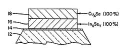 Fig 3a: Showing the 2 stage deposition of layers 16 (InxSey) at 100% followed by layer 18 (CuxSe) at 100% which will homogenize at temperature to form CuInSe2
 -
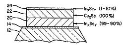 Fig 3b: An alternate showing 3 stage deposition of layer 20 (InxSey) at 99-90% followed by layer 22 (CuxSe) at 100% and then appling layer 24 (InxSey) at 1-10%
 -
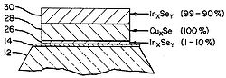 Fig 3c: Another alternate showing 3 stage deposition of layer 26 (InxSey) at 1-10% followed by layer 28 (CuxSe) at 100% and then appling layer 30 (InxSey) at 90-99%


The size of the substrate will dictate the size of the deposition chamber. This provides an opportunity for the manufacturers to save money and resources by selecting only chambers that fit the needs of their chosen substrate sizes. In cases where the evaporation area exceeds the size of the substrate, there is a notable loss of material to this area. It is impossible to completely control the evaporated material flow, but it is forced toward a cooler substrate in hopes of properly condensing the material, thus the process lacks the ability to utilize all material. This material collects in areas like the chamber walls, the conveyor system which the substrate travels, and can be collected in any surfaces other than the substrate.
An opportunity exist to develop a better way to reclaim this material other than the dis-assembly and removal of the chamber. Work in this area is very limited and often the chamber components are removed to be cleaned by using chemical bath techniques.
Upon manufacture of the CIGS layer, material deposition on the substrate causes over spray. A copper film layer will be lined in the deposition chamber to collect over spray. The copper film will be produced at the recycling facility and then taken to the manufacturing facility to integrate into the deposition process. Collection plates will then return to recycling facility and separated via the smelting process.
End of life module recycling
The recycling of end of life modules will become an increasing concern as the production of PV modules increases with demand. The continued improvement of thin-film cells will likely bring CIGS modules into a larger part of the market. With this increase, the demand for recycling will also increase and provide an opportunity to recycle as opposed to disposing the material in landfills. Complications from the material chemistry may cause modules to become hazardous after their usable life.

The processing of modules into recycled materials has been designed around removing as much of the mass material as possible, ideally the recycling of the cells frame, glass or backing components, and the attached electrical units. This process is best described as a deconstruction of the cell into its parts and leaving the semiconductor materials together in a processable unit.
The frame and electrical components can simply be removed and separated by hand. Thus the cost would be an hourly wage which could be estimated by measuring the kilograms of material processed per hour(kg/hr).
The material is then recycled using one of two methods to collect the precious metals. The first method would be a physical and chemical separation process, using multiple steps to break down the materials into smaller particles. The other would be a smelting process designed to extract metals from ore. Depending on space and capital investments, the best method may be determined by cost benefit.
Using the physical and chemical separation technique, the material can be further processed to get the materials separated into smaller and smaller particles. Accomplishing this task will take the use of machines that can physically, chemically, or thermally remove the metals from the glass or plastics used in the backing or cover slides of the cells. An effective way to perform the separation would be the use of a hammer mill that could crush, grind, and screen the material into smaller particles. Metals can be removed from the crushed glass by chemical dissolution or electrodeoposition.[18] Choosing a proper screen to sort the material can be determined through research or experimentally. Metal, glass, and any Ethylene-vinyl acetate (EVA) can be separated using chemical additives. The first material removed by screening will be the EVA which leaves the metal and glass particles. The metal sludge and large glass particles can be separated using the proper screen. The larger glass particles are then sent to be recycled. Further separation of the metal and small glass particles can be done using Hydro-metallurgical separation.[18]
Collection methods for retired CIGS solar cells can be quantified in terms of energy used by the hammer mill, because dis-assembly of the solar cells is performed by hand so, energy cost is not measurable. Hammer mill electric motors are estimated at 150 horsepower[19] () and run 4 hours a day. Physical Solar Cell dis-assembly was estimated at 1 m2 every 10 minutes, or 6 m2 every hour. Energy cost of collection methods is calculated to be 1.74 kW-hrs/g as shown:
In a more condensed method, the use of a smelting unit provides all the recycling in one multi-action step. Often using smelting in the extraction of iron ore, the material from the PV cells can be shredded into a smelting unit and then processed at high temperatures. Silica from the glass can be used in the smelting process in order to provide a fluxing agent and to trap heat to produce more efficient energy during the process. The glass portion of the material would be consumed in this flux and provide an easy way to recycle the glass by using it as a flux agent. Rates from literature estimate the cost of this process at around $185/ton.[18] The Process then uses anodes in the smelting furnaces to collect the copper and the metals that dissolve into it. Any metals that do not dissolve into the copper can be separated and collected in waste streams. Estimated cost from research for CIGS recycling in this manner is $0.08/W with use of municipal collection.[18][20]
An other separation methodis presented in figure 2 to illustrate steps to recycle CIGS-based thin-film module.

Firstly, To remove and collect metal frames and junction box with cable manually. Then Separate the cover glass by heating the CIGS-based thin-film module and mechanically pushing the soda-lime glass in horizontal direction. Remove residual EVA on the surface of CIGS-based device part by immersing in an acetic acid solution to collect a residual device part consisted of CIGS based absorber/ MO base electrode/ soda-lime glass. After that, collect the CIGS-based absorber part as metal powder by a mechanical scribing technique. Finally collect the soda-lime glass by dissolving the MO layer with a diluted nitric acid solution.
Waste recycling method for CdS buffer layer

A recycling method[22] for reducing CdS buffer layer waste was introduced. The CdS buffer layer for CIGS-based solar cells is grown in an aqueous solution containing a cadmium salt, ammonia, and thiourea. Bottlenecks of this technique called chemical bath deposition (CBD) are the low material yield and the production of toxic CdS containing waste. To improve yield and reduce waste, the CdS precipitate was separated from the waste after deposition by ultra-filtration and the permeate, which contains ammonia and thiourea, was used for the next CBD process after addition of cadmium salt. A simple schematic is seen on figure 3.
Purification of Semiconductor Materials

Most semiconductor devices require carefully controlled amounts of doping impurities in the material to achieve a specific resistivity. The material purity must then be maintained at a certain level before the final processing of the materials. These impurities affect the electrical conductivity of the semiconductor and the lifetime of the material. Other impurities are electrically inert and may be present in large quantities (approximately 0.3 to 20 parts per million atomic).[24]
All semiconductor materials must undergo extensive purification before they can be used in manufacturing of devices. The purity of copper must be 99% pure, indium must be 99.9% pure, gallium must be 99.99% pure, and selenium must be 99.9% pure.[25] Many purification processes can be repeated, so any waste material may be recycled through the same process several times. Copper and indium may be separated using metallurgical methods. Separation using metallurgical methods is done by heating the material to a solid+liquid phase, as shown in the phase diagram in Figure 6, and removing the frozen solid. Usually the frozen portion has fewer impurities.[24] Another economical method of removing impurities in gallium or copper is though electrorefining, which is a similar process to electrowinning. An electrowinning recovery system can recover metals from solutions which contain dissolved precious metals.[26] Literature search yields an energy quantification of 1.65 kw-hrs/kg.[27]
Literature search yields an energy quantification of the electro winning process, winning 1000 tons per year[28] and running at 500 amps and 220V.
Characterization of Materials
X-ray photoelectron spectroscopy (XPS) can be used as a characterization and metrology method for ultra-thin films in the semicondcutor processing industry. XPS has been implemented as a measurement tool for thickness, composition, and depth profiling of semiconductor materials.[29] Differential Scanning Calorimetry (DSC) can then be used to determine the purity of an element.[30]
In the purification process, the mass of element can be obtained as
Where MA is the mass of element A, M is the total mass of the waste of CIGS, and XA is the mass fraction of the element in the waste block, which is obtained with XPS.[29]
After the purification process, pure material of each element is obtained. The efficiency of the purification method is found
Where QA is the efficiency of purification, MAQ is the mass of element A after purification.
Then the purity of the obtained element can be found using Differential scanning calorimetry..[30]
Recycling Plant Design
[edit | edit source]Equipment Summary
Hammer Mill
- 1.74 kW∙hr/g
- 0.9 m2
Smelter
- 1.65∙10-3 kW∙hr/g
- 14 m2
Electrowinning Recovery System
- 1.06∙10-3 kW∙hr/g
- 9.3 m2 Surface Area[26]Total Recycling Plant Energy
- 15.2 Gigawatts
Total plant energy is calculated assuming 20 units of each piece of equipment listed in the summary for large scale production.
Co-Location
Ideally, the most effective location for a CIGS recycling plant would be near an LCD manufacturer. LCD's contain Copper, Indium, and Gallium in the processing techniques. Crystalfontz America in Spokane Valley, Washington is a great location to recycle valuable materials from the solar cells. A schematic for a possible industrial co-location is represented in figure 7. End of life modules are put into Glass-metal separating process, in which glass is sent to a sheet glass factory, Aluminium is sent to aircraft wing factory after purification, and semiconductor is put into semiconductor recycling plant. EVA, which is a polymer cover for the solar cell panel can be reproduced as fuel in fuel factory. The fuel is send to transportation station for use. Photovoltaic plant collect raw materials from semiconductor recycling plant and sheet glass factory as well as aluminium factory, can produce new CIGS-based thin film solar cell. The waste materials during the process can also be sent to semiconductor recycling plant for recycling. All heat generated by factories above can be used to ether supply worker life or sent to green house.

Alternatives to Recycling or Downcycling
This is in the worst case scenario where the ability to collect the materials and bring them to the solar cell purity needed to make CIGS modules. This should not be a process relied upon by recyclers due to the constant impurity of the material until the quality no longer constitues recycling. The goal of our process is to purify the materials into at least 5N purity for use in other electronics or for reuse in CIGS modules.
The primary use for copper indium gallium diselenide is photovoltaic solar cells. Quantification of materials was found through a literature search having values of 33-40 g/m2 and 3.03x10⁻⁷ g/Wpeak[31] Production of CIGS solar cells only yields 40% of the material deposited onto the substrate, leaving 60% for waste.[4]From a literature, it is estimated the collection ratio can be up to 93%[21] for the absorber.
This provides an opportunity for a large amount of waste material to be collected and recycled. Waste material can be collected and processed to individual elements and re-sold for other uses.
- Cover glass, which is the most expensive part in this module, is supplied as a raw material for the glass industry. Especially for the creation of new substrate.
- EVA as pottant can be reused as a kind of fuel.
- Zinc acetate solution is under investigation on the possibility to reuse as the chemical source for ZnO-based high-resistivity buffer layers at the chemical bath deposition step.
- Metal powder of the CIGS-based absorber can reuse as one of the chemical resource for CIGS-based absorbers by both coevaporation and selenization/sulfurization.
- Mo-rich sluge is supplied to the non-ferrous metal refining industry.
- Selenium can be used to decolorize glass, it is also used in anti-dandruff shampoo. Selenium is removed from CIGS by reduction processing prior to our smelting process.
- Indium is a high demand, rare material that is used in LCD screens. Indium can be removed from CIGS waste material using a liquid-liquid Baysolvex D2EHPA extractant (di(2-ethylhexyl)phosphoric acid).
- Gallium is used in the production of LED's and is extracted using liquid-liquid extraction.[7]
The pros and cons using alternative recycling methods instead of producing modules using recycled material are:
Pros
- Higher Demand
Cons
- Not as lucrative use of copper and selenium
- Not as environmentally friendly
Safety Plan
- Each plant occupant requires proper Personal Protective Equipment.
- Safety Glasses
- Gloves
- Face Shields
- Safety Boots
- Flame Retardant Jacket
- Hood Vents:
- Melting Process
- Electrowinning
- Safety training
- Fire Evacuation
- Hazardous Chemical
- Hazardous chemical and communication posters throughout plant containing clean up procedure
MSDS binder containing the following:
Copper - http://web.archive.org/web/20180123230121/http://www.sciencelab.com:80/msds.php?msdsId=9923549
Indium - http://web.archive.org/web/20170503015204/http://www.sciencelab.com:80/msds.php?msdsId=9924359
Galium - http://web.archive.org/web/20170503015157/http://www.sciencelab.com:80/msds.php?msdsId=9924116
Selenium - http://web.archive.org/web/20181011174639/http://www.sciencelab.com:80/msds.php?msdsId=9924874
Cadmium Sulfide - http://web.archive.org/web/20170430012843/http://www.sciencelab.com:80/msds.php?msdsId=9923232
Zinc Oxide - http://web.archive.org/web/20181013230023/http://www.sciencelab.com/msds.php?msdsId=9927329
Molybdenum - http://web.archive.org/web/20150105121350/http://www.molybdenum.com:80/health.pdf
Aluminum - http://web.archive.org/web/20181127014751/http://www.sciencelab.com:80/msds.php?msdsId=9922844
Crushed Lime Glass - http://web.archive.org/web/20120113042939/http://www.hunterproducts.com:80/glass_beads.pdf
Ethylene Vinyl Acetate - http://web.archive.org/web/20120916122028/http://www.arkema-inc.com/plants/canada/msds/AP2800.pdf
Acetic Acid - http://web.archive.org/web/20181208153211/http://www.sciencelab.com:80/msds.php?msdsId=9922769
Thiourea - http://web.archive.org/web/20181003200157/http://www.sciencelab.com:80/msds.php?msdsId=9927297
Material Flow Diagram
CIGS scrap material will be collected and separation of Indium, Gallium, and Copper from Selenium. Selenium is electrowon to increase purity. Gallium is separated from Indium and Copper and Gallium impurity is further increased by electrowinning. Indium and Copper is separated metallurgically and each individiual element is further purified through the electrowinning process. This process is shown in Figure 8.
References
[edit | edit source]- ↑ A.V. Naumov, Selenium and Tellurium: State of the Markets, The Crisis, and its Consequences. Metallurgist, Vol.54, Nos. 3-4, 2010
- ↑ A. Rocket, R.N. Bhattacharya, C. Eberspacher, V. Kapur, S. Wei "Basic Research Opportunities in Cu-Chalcopyrite Photovoltaics", 1999.
- ↑ 3.0 3.1 3.2 M.A. Contreras, K. Ramanathan, J. Abushama, F. Hasoon, D.L. Young, B. Egaas, and R. Noufi, Prog. Photovoltaics 13 (2005) p. 209
- ↑ 4.0 4.1 Osborn, September 27th, 2010 http://www.pv-tech.org/product_reviews/umicores_cigs_production_scrap_recycling_closes_the_materials_loop
- ↑ 5.0 5.1 Glass on Web,(2008). http://web.archive.org/web/20110820053112/http://www.glassonweb.com/articles/utils/print.php?id=543
- ↑ A.M. Gabor, J.R. Tuttle, D. S. Albin, M. A. Contreras, and R. Noufi, Appli. Phys. Lett. 65, 198 (1994).
- ↑ 7.0 7.1 http://www.sense-eu.net/fileadmin/user_upload/intern/documents/Results_and_Downloads/SENSE_Recycling.pdf
- ↑ N. C. Mcdonald, J. M. Pearce,Producer responsibility and recycling solar photovoltaic modules, Energy Policy, Volume 38, Issue 11, November 2010, Pages 7041-7047
- ↑ K. Zweibel, Sol. Energy Mater. Sol. Cells 59 (1999) 1.
- ↑ Kushiya, K., 2003. Progress in large-area Cu(In,Ga)Se2-based thin-film modules with the efficiency of over 13%. In: Proceedings of the 3rd WCPEC, Osaka, Japan, pp. 319–324.
- ↑ 11.0 11.1 Markus E. Beck, Michael Cocivera, Thin-film copper indium diselenide prepared by selenization indium oxide formed by spray pyrolysis, Thin Solid Films, 272(1996)71-82.
- ↑ Bhattacharya, R.N., Hiltner, J.F., Batchelor, W., Contreras,R.N., Noufi, R.N., Sites, J.R., 2000. 15.4% CuIn1�xGaxSe2-based photovoltaic cells from solution-based precursor films. Thin Solid Films 361, 396–399.
- ↑ Hariklia (Lili) Deligianni, Shafaat Ahmed, and Lubomyr T. Romankiw, The Next Frontier: Electrodeposition for Solar Cell Fabrication.http://www.electrochem.org/dl/interface/sum/sum11/sum11_p047-053.pdf
- ↑ Duchemin, S., Bougnot, J., El Ghzizal, A., Belghit, K., 1989. Studies on the improvement of sprayed CdS–SuInSe2 solar cells. In: Palz, W., Wrixon, G.T., Helm, P. (Eds.), Proceedings of the 9th EPVSEC, Freiburg, Germany, pp. 476–479.
- ↑ Kapur, V.K., Bansal, A., Le, P., Asensio O., Shigeoka N., 2003b. Non-vacuum processing of CIGS solar cells on flexibe polymeric substrates. In: Proceedings of the 3rd WCPEC, Osaka 2003, Japan, pp. 465–468.
- ↑ M. Kaelin, etc. Low-cost CIGS solar cells by paste coating and selenization. Thin Solid Films Volumes 480-481, 1 June 2005, Pages 486-490. http://www.sciencedirect.com/science/article/pii/S0040609004015597
- ↑ M. Kemell, M. Ritala, M. Leskela, "Thin Film Deposition Methods for CuInSe2 Solar Cells" (2005).
- ↑ 18.0 18.1 18.2 18.3 18.4 Fthenakis, V. M. (2000). End-of-life management and recycling of PV modules. Energy Policy 28, 1051-1058.
- ↑ Bliss Industries http://web.archive.org/web/20180403150658/http://www.bliss-industries.com:80/system/resources/0000/0059/condmill.pdf
- ↑ Fthenakis, V. M. (1996). Recycling Strategies to Enhance the Commercial Viability of CIS Photovoltaics. Progress In Photovoltaics: Research and Applications,vol. 4, 447-456.
- ↑ 21.0 21.1 Katsumi Kushiya, etc. DEVELOPMENT OF RECYCLING AND REUSE TECHNOLOGIES FOR LARGEAREA Cu(1nGa)Sez-BASED THIN-FILM MODULES. 3rd World Conference on Photovoltaic Energy Conversion. May 11-18, 2003 Osaka, Japan. http://ieeexplore.ieee.org/stamp/stamp.jsp?tp=&arnumber=1306308
- ↑ 22.0 22.1 D. Hariskos, M. Powalla. Chemical bath deposition of CdS buffer layer: prospects of increasing materials yield and reducing waste. Thin Solid Films 387(2001). 179-18
- ↑ U.S. Patent #5,441,897, Noufi et al.,METHOD OF FABRICATING HIGH-EFFICIENCY CU(IN,GA)(SES)2 THIN FILMS FOR SOLAR CELLS, AUG. 15,1995.
- ↑ 24.0 24.1 McKetta, John J., and William A. Cunningham. "Semiconductor Material Purification." Encyclopedia of Chemical Processing and Design. New York: M. Dekker, 1976. 344-45. Print
- ↑ Retrieved Oct. 6 2011, Geller Micro analytical Laboratory, Inc. http://www.gellermicro.com:80/standards/uhv-el.htm
- ↑ 26.0 26.1 Retrieved Oct. 6, 2011, Allied Plating Supplies, Inc. http://www.alliedplating.com/store.asp?pid=18509
- ↑ retrieved Oct 6 2011,Institute for Energy and Environment, Chapter 7 http://www.ieer.org/reports/climchg/ch7.pdf
- ↑ retrieved Oct 6 2011,Electro Refining of Copper http://web.archive.org/web/20120309040049/http://mech2006.vtk.be/downloads/mech2005/2e/materiaalkunde/5-b%20copper.pdf
- ↑ 29.0 29.1 Brundle, C.R., Conti, G., Mack, P. (2010). XPS and Angle Resolved XPS, in the Semiconductor Industry: Characterization and Metrology Control of Ultra-Thin Films.
- ↑ 30.0 30.1 C. Plato and S. R. Glasgow. (1969) Anal. Chem., 41 (2), 330.
- ↑ Otte,Makhova,Braun,Konovalov "Flexible Cu(In,Ga)Se2 thin-film solar cells for space application" 2006 http://www.sciencedirect.com/science/article/pii/S0040609005022856
- ↑ Retrieved October 6, 2011, from Nexteck Quality and Service: http://www.nexteck-corp.com:80/eng/product-cigs.html
| Authors | |
|---|---|
| License | CC-BY-SA-3.0 |
| Organizations | MTU |
| Cite as | Binghan, Tbotbyl, Dmmacewe, ATuthill (2011–2026). "Semiconductor recycling plant case study of CIGS photovoltaic manufacturing". Appropedia. Retrieved June 6, 2026. |