No higher resolution available.
Layers.png (676 × 458 pixels, file size: 72 KB, MIME type: image/png)
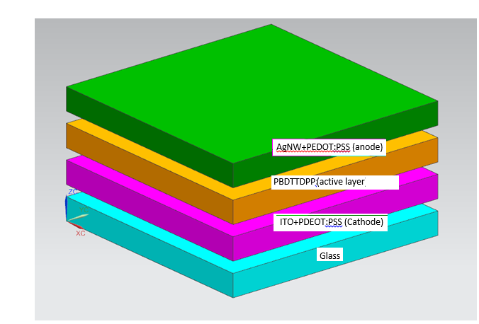
Layers of our semiconductor in order of what they are printed on the glass mold in 100 nm. thickness sections. The separation in layer within image is not in actual semiconductor just for imaging purposes.
File history
Click on a date/time to view the file as it appeared at that time.
| Date/Time | Thumbnail | Dimensions | User | Comment | |
|---|---|---|---|---|---|
| current | 01:47, 16 October 2013 | | 676 × 458 (72 KB) | Jgponton (talk | contribs) | |
| 00:40, 16 October 2013 | 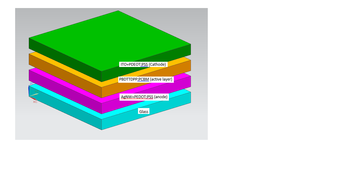 | 1,166 × 596 (69 KB) | Jgponton (talk | contribs) | Layers of our semiconductor in order of what they are printed on the glass mold in 100 nm. thickness sections. The separation in layer within image is not in actual semiconductor just for imaging purposes. |
You cannot overwrite this file.
File usage
The following page uses this file: