The current logo, used since 2005.
Project data
Authors Emily Wolbeck
Matthew Tianen
Travis Hepfner
Location Michigan, USA
OKH Manifest Download

This is a speculative class project and needs to be refined before being deployed at any scale.

In 1968, scientists, Robert Noyce and Gordon MooreW, founded Intel with a vision for semiconductor memory products. By 1971, they had introduced the world's first microprocessor.[1]

Type of Semiconductor and How it's Made

[https://en.wikipedia.org/wiki/File:Monokristalines Silizium für die Waferherstellung.jpg Monocrystalline silicon ingot grown by the Czochralski process
mqdefault.jpgYouTube_icon.svg

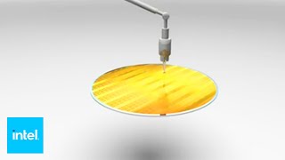
Intel video explains how semiconductors are created. How it's Made

Growth of Market

Type of Market

Intel has a wide variety of customers from home users to worldwide organizations. Here is a list customers that Intel itself lists on its website with links to the provided programs that Intel offers to each of their clientele.

Embedded Customers
Hardware Developers
Intelligent Systems Customers
IT Managers
Resellers
Small Business
Software Developers
Investors and Financial Analysts
Educators
Gamers
Home Users

Current Recycling Practices

How?

What components?

Amount of Semiconductor

Methods of collecting the lost semiconductor materials

Viability

Post-Consumer Recycling

Collection Methods

For example, in 2011, IBM's PELM operations worldwide processed over 37,950 metric tons of end-of-life products which was about 97.6 percent of the total amount processed recycled.[12] Since we are only focusing on processors from Intel for this project we will use the estimate of 97.6 percent for our 46,700kg (the total silicon weight in processors for 2010) to estimate the amount of silicon recovered. This gives us a total of 45,579.2kg of estimated silicon that can be saved from these processors per year. We plan on collecting the processors by providing free recycling to consumers. In cooperation with Intel the customer would send their processor(s) in to Intel. As a third party, we would then either purchase or have Intel donate their scrap wafers and the CPU's that consumers sent in by mail to our program. By parterning with Intel we believe that we would receive around 90% of the total processors produced in a year. If there is an estimated 67,040,000 Intel CPU's made per year 60,336,000 would be returned to our company. Multiplying by the amount of silicon in an average CPU (.697g) then we would able to recycle around 42054kg of pure Si per year. We would also build our plant next to Intel's so that shipping between the plants can be ignored

Contaminants

Table 1. Typical impurity concentrations found in electronic-grade silicon (EGS).[15]

Element Concentration (ppb)
arsenic < 0.001
antimony < 0.001
boron ≤ 0.1
carbon 100-1000
chromium < 0.01
cobalt 0.001
copper 0.1
gold < 0.00001
iron 0.1-1.0
nickel 0.1-0.5
oxygen 100-400
phosphorus ≤ 0.3
silver 0.001
zinc < 0.1

Purification Methods

Characterization Methods

There are a few different ways you can characterize a silicon based semi-conductor. There is the Electrical characterization, the optical characterization, and the physical/chemical characterization.

Electrical characterization helps you determine the resistivity, carrier concentration, mobility, contact resistance, barrier height, depletion width, oxide charge, interface states, carrier lifetimes, and deep level impurities. Two-Point Probe, Four-Point Probe, Differential Hall Effect, Capacitance-Voltage Profiling, DLTS, and DLCP.

Optical characterization includes microscopy microscopy, ellipsometry, photoluminescence, transmission spectroscopy, absorption spectroscopy, raman spectroscopy, reflectance modulation, cathodoluminescence. There are still alot of other methods out these are merely an example of some of the tools available.

Physical/Chemical characterization techniques utilize ion beams X-rays, and electron beams to measure the physical characteristics of the semiconductor. these include (electron Beam) SEM, TEM, AES, EMP, EELS, (Ion Beam) Sputtering, SIMS, RBS, (X-rays) XRF, XPS, XRD, X-ray topography Neutron Activation Analysis (NAA) Chemical Etching.

Since we are trying to utilize the silicon from these processors for use in photovoltaic cells it makes clear sense to utilize the electrical characterization of the materials involved. The other characterization methods were included merely to illustrate how many different ways there is to show how a semiconductor can be tested to determine exactly what it's exact composition is. This will basically be used to confirm the information that would be obtained from Intel as far as the type of silicon used in their processors. Sadly this information is proprietary so we don't know anything other than the average purity of silicon for processor use. thankfully the purity for this application is significantly higher than that needed for use in a photo voltaic cell.

Energy Needed for Recycling

To keep the energy needed to transport a wafer to our facility we will be locating it next to an Intel plant that receives waste processors. Those would then be obtained put through the entire process of recycling them. Information regarding the actual energy used by individual machines that actually handle these processor dies is very hard to come by and not made publicly available. However there is a wealth of information about the energy savings involved in wafer reclamation processes. IBM claims that depending on the process, it can save between 30% and 90% of the energy used to produce wafers from scratch.[20] It takes 2130 kWh to produce one kilogram of single crystal silicon from scratch.[21] With a conservative estimate of 50% energy saving, this could result in 1065 kWh per kilogram for the reclamation portion of the process. Using a ZT-90D directional solidification furnace we a 90 kg crucible capacity, the energy required would be 73 kWh per kilogram.[22] This results in a total energy of 1138 kWh per kilogram of silicon for all of the processing steps combined.

Alternatives to Straight Recycling

Now say you have a processor that is having hardware issues and cannot function anymore. You could grind off the old transistors and any circuitry to then redeposit new circuitry onto the dies. Even though this is possible it doesn't mean that it is really feasible, since you would have to retool each individual die by itself. We believe the best process would be to merely remove the impurities from the dies and utilize the silicon for the creation of photo-voltaic cells. Since the silicon already exceeds the purity level needed for solar cells, further purification will not be required. The following statement alludes to the use of full scrap wafers already being utilized for the creation of solar cells.

Semiconductor Recycling Facility

Equipment and Processing

  1. Chemical Stripping OrcaTM Automated Wet Process System will chemically strip the processors of contaminants.
  2. Surface Grinder Waida Super Precicion Surface Grinder will grind all remaining electronics on the processor off.
  3. Cleaning Process OrcaTM Automated Wet Process System will then wash away all excess contaminates that remain from griding.
  4. Melting in Furnace Polycrystalline Silicon Casting Furnace will then melt all the pure silicon into ingots which will then be trimmed to form blocks.

Safety Plan

The Occupational Safety and Health Administration (OSHA) is an organization with the United States Department of Labor. The recycling facility described above will follow all OSHA requirements. More information on OSHA regulations can be found on their website at http://www.osha.gov/.

Material Safety Data Sheets (MSDS)

Material Safety Data Sheets are required for all chemicals that enter the plant and will be placed in easily accessible to all employees. A list of the primary materials used in this recycling process, along with links to their MSDS, can be found below.

Safety Training

The recycling facility will have a Safety Training Program. The purpose of this program will be to train new employees on current and long-term safety issues as well as continue to provide continuing safety training to all employees. The Safety Training Program will focus on, but not limited to the topics below:

Semiconductor Material Flow Diagram

The following Flow Diagram outlines the workflow in the recycling plant. While the file is not a Dia file as requested, we were not able to download the Dia program onto the school computers and decided that Visio was the best alternative.

References

  1. ↑ Intel Company Information http://www.intel.com/content/www/us/en/company-overview/company-facts.html
  2. ↑ From Sand to Silicon"Making of a Chip" http://download.intel.com/newsroom/kits/chipmaking/pdfs/Sand-to-Silicon_45nm-Version.pdf
  3. ↑ The Economist http://www.economist.com/node/21542402
  4. ↑ Intel Corporate Resonsibility http://www.intel.com/content/www/us/en/corporate-responsibility/eco-responsible-operations.html
  5. ↑ List of Intel Microprocessors http://en.wikipedia.org/wiki/List_of_Intel_microprocessors
  6. ↑ Intel Webpage
  7. ↑ Intel from Sand to Silicon http://download.intel.com/newsroom/kits/chipmaking/pdfs/Sand-to-Silicon_22nm-Version.pdf
  8. ↑ "Analysis: Smart logic: Samsung chips away at Intel lead" Reuters http://web.archive.org/web/20150329123759/http://www.reuters.com/article/2012/06/21/us-chips-samsung-idUSBRE85K1OM20120621
  9. ↑ IBM http://www-935.ibm.com/services/us/gts/flash/burlington/
  10. ↑ ITJungle http://web.archive.org/web/20160414142512/http://www.itjungle.com/bns/bns103107-story01.html
  11. ↑ Computer Recycling http://en.wikipedia.org/wiki/Computer_recycling
  12. ↑ IBM http://www.ibm.com/ibm/environment/products/recycling.shtml
  13. ↑ Hazardous Waste Overview http://web.archive.org/web/20140722063645/http://seshaonline.org:80/scholarships/Hazardous_Waste_Overview.ppt
  14. ↑ http://cnx.org/content/m16530/latest/
  15. ↑ http://cnx.org/content/m16530/latest/
  16. ↑ http://www.microtechprocess.com/pdf/MTS_Reclaim.pdf
  17. ↑ http://web.archive.org/web/20140925010304/http://www.poseidonsolar.com:80/our-services/semiconductor-rejects-reclaim.html
  18. ↑ http://www.greenrhinoenergy.com/solar/technologies/pv_manufacturing.php
  19. ↑ http://www.kgbconsultingltd.com/downloads/Waste_Not_Want_Not.pdf
  20. ↑ http://www.renewableenergyworld.com/rea/news/article/2007/10/from-silicon-trash-to-solar-energy-50443
  21. ↑ http://books.google.com/books?id=5cqtnwkpybIC&pg=PA479&lpg=PA479&dq=silicon+wafer+reclamation+energy+usage&source=bl&ots=pzKlNDM5po&sig=2oVXBoo31WFnA_BCRgbvY5azqi0&hl=en&sa=X&ei=32R7UO-RMMjnyAGF9oCIBA&ved=0CCoQ6AEwAzgK#v=onepage&q&f=false
  22. ↑ http://efmpt.com/display.asp?bookid=1511
  23. ↑ http://www.azom.com/news.aspx?newsID=10379
  24. ↑ https://www.seton.com/resource-center/
  25. 1 2 3 4 http://www.sciencelab.com/msds
  26. 1 2 3 https://www.seton.com/resource-center/
Page data
Part of MY3701
Keywords recycling, semiconductors, Intel Processors
SDG SDG12 Responsible consumption and production
License CC-BY-SA-3.0
Organizations MTU
Language English ()
Translations Korean, Indonesian, Vietnamese, Spanish
Related 4 subpages, 10 pages link here
Views 8,822 page views (analytics)
Created September 28, 2012 by Emily Wolbeck
Last edit November 28, 2025 by Maintenance script