This is a speculative class project and needs to be refined before being deployed at any scale.
In 1968, scientists, Robert Noyce and Gordon MooreW, founded Intel with a vision for semiconductor memory products. By 1971, they had introduced the world's first microprocessor.[1]
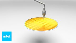
Type of Semiconductor and How it's Made

- Intel processors use 99.9999% pure silicon to make their wafers. The silicon is grown from melt into a large single crystal ingot. Wafers with a diameter of 300mm are cut from the ingot. After the wafers are polished and prepared, transistors are deposited on the surface. The processor dies are then cut from the wafer.[2]
Growth of Market
- Intel, is responsible for many of the advances that have made today's semiconductors possible. In the first nine months of 2011, the company generated $40.1 billion in revenue and $13.2 billion in pre-tax profit. Intel has no real rival in the market for chips that power PCs and servers.[verification needed] The firm's top brass attributes much of the company's success in harnessing this virtuous circle to the fact that it both designs and makes its chips, with ten chip factories ("fabs" in industry argot) operating and two more under construction. Brian Krzanich, Intel's manufacturing head, says this means it can bring chips to market faster and with fewer faults than rivals who use external firms, known as "foundries", to make their chips. This helps explain why it dominates the market for high-performance processors in PCs and servers.[3]
Type of Market
Intel has a wide variety of customers from home users to worldwide organizations. Here is a list customers that Intel itself lists on its website with links to the provided programs that Intel offers to each of their clientele.
- Business Use
- Embedded Customers
- Hardware Developers
- Intelligent Systems Customers
- IT Managers
- Resellers
- Small Business
- Software Developers
- Investors
- Education
- Personal Use
Current Recycling Practices[edit | edit source]
How?
- Intel's website discusses their various recycling practices. They are very active recyclers, claiming to reuse their waste water and avoid waste in their production processes.[4] Intel, however, has no apparent program for the recycling of processors or the semiconductors that they contain. Since they are outspoken about their recycling practices but silent about semiconductor recycling, it is assumed that no such program exists.
What components?
- We will be focusing on Central Processing Unit which is the brain of the computer. However Intel has created a lot of other types of processors through the course of the company's history. From the first 4 bit processors created in 1971, all the way up to the modern 64 bit Itanium 2 processor created in 2002, Intel has been constantly on the leading edge of innovation for chip creation.[5]
Amount of Semiconductor[edit | edit source]
- Processor dies for the Intel i7 have an area of 263 mm2.[6] The wafers used to create the dies are about 1 mm thick.[7] Given silicon's density of 2.65 g/cm3, one processor die with a volume of 263 mm3 (.263cm3) would have about.697g of high purity silicon. It is estimated that about 80% of all PCs have Intel processors in them.[8] If 83,800,000 computers were sold in 2010 then it can be estimated that about 67,040,000 of them contained an Intel processor. Multiplying that number by the amount of silicon in one processor gives a very rough estimate of the amount of silicon put into processors in a year. This comes out to be about 46,700kg of silicon per year.
- This amount seems significantly low considering the amount of silicon produced each year for the electronics industry (thousands of metric tons). However, there is no market data for how many units are sold. All data available are related to the revenue earned from processors. With no information available about units sold, it may be impossible to know exactly how much silicon is available in the market. Still, it seems likely that the real value is higher than the stated estimate.[verification needed]
Methods of collecting the lost semiconductor materials[edit | edit source]
- The Semiconductor Industry Association says that around 250,000 silicon wafers are started each day in the world, and IBM estimates that about 3.3 percent of the wafers are scrapped. By recycling those scrapped wafers at the Burlington facility[9] as monitor wafers, IBM saved more than $500,000 in 2006 and is projected to save $1.5 million in 2007 and that much each year going forward. IBM did not say how much money it could make selling the second-hand wafers. And by using recycled silicon, solar cell manufacturers can save between 30 percent and 90 percent of the energy they normally expend creating solar cells, those lowering the carbon footprint of their products.[10] However Intel has no obvious program for recycling their semiconductors and there is no real information on how semiconductors are currently being recycled because the processes are most likely protected by patents.
Viability[edit | edit source]
- We have decided to utilize Choice A (yes) Post-Consumer Recycling.
- We can use post-consumer semiconductor based processor for use in other semiconductors particularly for use in photo voltaic cells. With the extraction of the semiconductors (specifically silicon) from processors foreign contaminates will inevitably penetrate the pure silicon. Because photo voltaic cells don't require pure silicon to work properly the recycled silicon will function proficiently in the solar cells. Computer components are collected worldwide already for many different components/elements, such as gold or platinum, making the collection of those semiconductors feasible.[11]
Post-Consumer Recycling[edit | edit source]
Collection Methods[edit | edit source]
For example, in 2011, IBM's PELM operations worldwide processed over 37,950 metric tons of end-of-life products which was about 97.6 percent of the total amount processed recycled.[12] Since we are only focusing on processors from Intel for this project we will use the estimate of 97.6 percent for our 46,700kg (the total silicon weight in processors for 2010) to estimate the amount of silicon recovered. This gives us a total of 45,579.2kg of estimated silicon that can be saved from these processors per year. We plan on collecting the processors by providing free recycling to consumers. In cooperation with Intel the customer would send their processor(s) in to Intel. As a third party, we would then either purchase or have Intel donate their scrap wafers and the CPU's that consumers sent in by mail to our program. By parterning with Intel we believe that we would receive around 90% of the total processors produced in a year. If there is an estimated 67,040,000 Intel CPU's made per year 60,336,000 would be returned to our company. Multiplying by the amount of silicon in an average CPU (.697g) then we would able to recycle around 42054kg of pure Si per year. We would also build our plant next to Intel's so that shipping between the plants can be ignored
Contaminants[edit | edit source]
- Typical corrosive wastes for processors include: Sulfuric Acid, Hydroflouric Acid, Phosphoric Acid, Nitric Acid, Ammonium Hydroxide, and Hydrogen Peroxide. These acids are used for etching, stripping and cleaning the wafers. Tetramethyl Ammonium Hydroxide is used as a positive photoresistant developer.[13]
- The requirements of extreme purity for electronic device fabrication require additional purification steps in order to produce electronic-grade silicon (EGS). In order for the purity levels to be acceptable for subsequent crystal growth and device fabrication, EGS must have carbon and oxygen impurity levels less than a few parts per million (ppm), and metal impurities at the parts per billion (ppb) range or lower(see table below). Besides the purity, the production cost and the specifications must meet the industry desires.[14] However because we are not planning on recycling our silicon wafers in electronics but in solar panels we can be a little more liberal with amount of contaminants in our silicon.
Table 1. Typical impurity concentrations found in electronic-grade silicon (EGS).[15]
| Element | Concentration (ppb) |
|---|---|
| arsenic | < 0.001 |
| antimony | < 0.001 |
| boron | ≤ 0.1 |
| carbon | 100-1000 |
| chromium | < 0.01 |
| cobalt | 0.001 |
| copper | 0.1 |
| gold | < 0.00001 |
| iron | 0.1-1.0 |
| nickel | 0.1-0.5 |
| oxygen | 100-400 |
| phosphorus | ≤ 0.3 |
| silver | 0.001 |
| zinc | < 0.1 |
Purification Methods[edit | edit source]
- Methods for reclamation of wafers from the electronics industry already exist. Wafers that have all electronics deposited can be cleaned, polished and reused.[verification needed] This process can also be used to clean existing processor chips which have the same surface properties as the uncut wafers.
- The processor chips are chemically treated to remove impurities.
- First they are treated in a mixture of sulfuric acid and hydrogen peroxide.
- Next is an etch in hydrofluoric acid followed by an alkaline etch using ammonium hydroxide or potassium hydroxide.
- The chips are then ground and polished to remove remaining surface features.
- Finally, residual particles are removed during a two stage cleaning process. The first step uses a mixture of water, hydrogen peroxide, and ammonium hydroxide and the second uses water, hydrogen peroxide, and hydrochloric acid. This process results in clean, pure silicon with a slight thickness reduction.[16] The thickness loss is up to 10 microns or about 1.5% of silicon.[17]
- Once the silicon is cleaned of impurities it can be melted down and cast into ingots of polycrystalline silicon and cut into square ingots for use in solar cells[18]
- Overall, very little silicon is lost. About 1.5% is lost during the cleaning process. Even assuming triple the thickness loss during cleaning to be conservative, only 4.5% of silicon is lost. There are also likely to be significant kerf losses from sawing. One source estimates 35% kerf loss during wafer production[19] but the dust from wafer cutting can be recycled back into melt for new ingots. It is likely that at least 95% of silicon could probably be recovered from this process.
Characterization Methods[edit | edit source]
There are a few different ways you can characterize a silicon based semi-conductor. There is the Electrical characterization, the optical characterization, and the physical/chemical characterization.
Electrical characterization helps you determine the resistivity, carrier concentration, mobility, contact resistance, barrier height, depletion width, oxide charge, interface states, carrier lifetimes, and deep level impurities. Two-Point Probe, Four-Point Probe, Differential Hall Effect, Capacitance-Voltage Profiling, DLTS, and DLCP.
Optical characterization includes microscopy microscopy, ellipsometry, photoluminescence, transmission spectroscopy, absorption spectroscopy, raman spectroscopy, reflectance modulation, cathodoluminescence. There are still alot of other methods out these are merely an example of some of the tools available.
Physical/Chemical characterization techniques utilize ion beams X-rays, and electron beams to measure the physical characteristics of the semiconductor. these include (electron Beam) SEM, TEM, AES, EMP, EELS, (Ion Beam) Sputtering, SIMS, RBS, (X-rays) XRF, XPS, XRD, X-ray topography Neutron Activation Analysis (NAA) Chemical Etching.
Since we are trying to utilize the silicon from these processors for use in photovoltaic cells it makes clear sense to utilize the electrical characterization of the materials involved. The other characterization methods were included merely to illustrate how many different ways there is to show how a semiconductor can be tested to determine exactly what it's exact composition is. This will basically be used to confirm the information that would be obtained from Intel as far as the type of silicon used in their processors. Sadly this information is proprietary so we don't know anything other than the average purity of silicon for processor use. thankfully the purity for this application is significantly higher than that needed for use in a photo voltaic cell.
Energy Needed for Recycling[edit | edit source]
To keep the energy needed to transport a wafer to our facility we will be locating it next to an Intel plant that receives waste processors. Those would then be obtained put through the entire process of recycling them. Information regarding the actual energy used by individual machines that actually handle these processor dies is very hard to come by and not made publicly available. However there is a wealth of information about the energy savings involved in wafer reclamation processes. IBM claims that depending on the process, it can save between 30% and 90% of the energy used to produce wafers from scratch.[20] It takes 2130 kWh to produce one kilogram of single crystal silicon from scratch.[21] With a conservative estimate of 50% energy saving, this could result in 1065 kWh per kilogram for the reclamation portion of the process. Using a ZT-90D directional solidification furnace we a 90 kg crucible capacity, the energy required would be 73 kWh per kilogram.[22] This results in a total energy of 1138 kWh per kilogram of silicon for all of the processing steps combined.
Alternatives to Straight Recycling[edit | edit source]
- Instead of straight recycling, which is the process of removing impurities and utilizing the raw silicon. You could also retool the processors to obtain continued work, however you will not be able to get this device to work as well as a new one. The rough process for working a die (individual processor) could possibly be done a couple of different ways. One if the processor still works it can be just used in new application. Say you have a calculator that needs a main processing unit you could utilize a computer processor that still works to run the calculator. This processor was originally meant to run a lot more than just the components of a calculator, but instead of being thrown out and/or destroyed it has found new life.
Now say you have a processor that is having hardware issues and cannot function anymore. You could grind off the old transistors and any circuitry to then redeposit new circuitry onto the dies. Even though this is possible it doesn't mean that it is really feasible, since you would have to retool each individual die by itself. We believe the best process would be to merely remove the impurities from the dies and utilize the silicon for the creation of photo-voltaic cells. Since the silicon already exceeds the purity level needed for solar cells, further purification will not be required. The following statement alludes to the use of full scrap wafers already being utilized for the creation of solar cells.
- The wafer reclamation process produces monitor wafers from scrap product wafers - generating an overall energy savings of up to 90%. When monitors wafers reach end of life they are sold to the solar industry. Depending on how a specific solar cell manufacturer chooses to process a batch of reclaimed wafers - they could save between 30 - 90% of the energy that they would have needed if they'd used a new silicon material source.[23]
Semiconductor Recycling Facility[edit | edit source]
Equipment and Processing
- Chemical Stripping OrcaTM Automated Wet Process System will chemically strip the processors of contaminants.
- Surface Grinder Waida Super Precicion Surface Grinder will grind all remaining electronics on the processor off.
- Cleaning Process OrcaTM Automated Wet Process System will then wash away all excess contaminates that remain from griding.
- Melting in Furnace Polycrystalline Silicon Casting Furnace will then melt all the pure silicon into ingots which will then be trimmed to form blocks.
Safety Plan[edit | edit source]
The Occupational Safety and Health Administration (OSHA) is an organization with the United States Department of Labor. The recycling facility described above will follow all OSHA requirements. More information on OSHA regulations can be found on their website at http://www.osha.gov/.
Material Safety Data Sheets (MSDS)
Material Safety Data Sheets are required for all chemicals that enter the plant and will be placed in easily accessible to all employees. A list of the primary materials used in this recycling process, along with links to their MSDS, can be found below.
- Sulfuric Acid[H2SO4 MSDS][24]
- Hydrofluoric AcidHF MSDS[25]
- Phosphoric Acid H3PO4 MSDS[25]
- Nitric Acid HNO3 MSDS[25]
- Ammonium HydroxideNH4OH MSDS[25]
- Hydrogen Peroxide[2(HO) MSDS][26]
- Hydrochloric AcidHCl MSDS[26]
- WaterH2O MSDS[26]
Safety Training
The recycling facility will have a Safety Training Program. The purpose of this program will be to train new employees on current and long-term safety issues as well as continue to provide continuing safety training to all employees. The Safety Training Program will focus on, but not limited to the topics below:
- How to read a MSDS
- Emergency Response: Hazardous Chemicals
- Review of Hazardous Chemicals
- How to prevent/clean-up spills
- How to properly label containers
- Procedures for handling chemicals
- Procedures for fire or large scale chemical spills
Semiconductor Material Flow Diagram[edit | edit source]
The following Flow Diagram outlines the workflow in the recycling plant. While the file is not a Dia file as requested, we were not able to download the Dia program onto the school computers and decided that Visio was the best alternative.

References[edit | edit source]
- ↑ Intel Company Information http://www.intel.com/content/www/us/en/company-overview/company-facts.html
- ↑ From Sand to Silicon"Making of a Chip" http://download.intel.com/newsroom/kits/chipmaking/pdfs/Sand-to-Silicon_45nm-Version.pdf
- ↑ The Economist http://www.economist.com/node/21542402
- ↑ Intel Corporate Resonsibility http://www.intel.com/content/www/us/en/corporate-responsibility/eco-responsible-operations.html
- ↑ List of Intel Microprocessors http://en.wikipedia.org/wiki/List_of_Intel_microprocessors
- ↑ Intel Webpage [1]
- ↑ Intel from Sand to Silicon http://download.intel.com/newsroom/kits/chipmaking/pdfs/Sand-to-Silicon_22nm-Version.pdf
- ↑ "Analysis: Smart logic: Samsung chips away at Intel lead" Reuters http://web.archive.org/web/20150329123759/http://www.reuters.com/article/2012/06/21/us-chips-samsung-idUSBRE85K1OM20120621
- ↑ IBM http://www-935.ibm.com/services/us/gts/flash/burlington/
- ↑ ITJungle http://web.archive.org/web/20160414142512/http://www.itjungle.com/bns/bns103107-story01.html
- ↑ Computer Recycling http://en.wikipedia.org/wiki/Computer_recycling
- ↑ IBM http://www.ibm.com/ibm/environment/products/recycling.shtml
- ↑ Hazardous Waste Overview http://web.archive.org/web/20140722063645/http://seshaonline.org:80/scholarships/Hazardous_Waste_Overview.ppt
- ↑ http://cnx.org/content/m16530/latest/
- ↑ http://cnx.org/content/m16530/latest/
- ↑ http://www.microtechprocess.com/pdf/MTS_Reclaim.pdf
- ↑ http://web.archive.org/web/20140925010304/http://www.poseidonsolar.com:80/our-services/semiconductor-rejects-reclaim.html
- ↑ http://www.greenrhinoenergy.com/solar/technologies/pv_manufacturing.php
- ↑ http://www.kgbconsultingltd.com/downloads/Waste_Not_Want_Not.pdf
- ↑ http://www.renewableenergyworld.com/rea/news/article/2007/10/from-silicon-trash-to-solar-energy-50443
- ↑ http://books.google.com/books?id=5cqtnwkpybIC&pg=PA479&lpg=PA479&dq=silicon+wafer+reclamation+energy+usage&source=bl&ots=pzKlNDM5po&sig=2oVXBoo31WFnA_BCRgbvY5azqi0&hl=en&sa=X&ei=32R7UO-RMMjnyAGF9oCIBA&ved=0CCoQ6AEwAzgK#v=onepage&q&f=false
- ↑ http://efmpt.com/display.asp?bookid=1511
- ↑ http://www.azom.com/news.aspx?newsID=10379
- ↑ https://www.seton.com/resource-center/
- ↑ 25.0 25.1 25.2 25.3 http://www.sciencelab.com/msds
- ↑ 26.0 26.1 26.2 https://www.seton.com/resource-center/