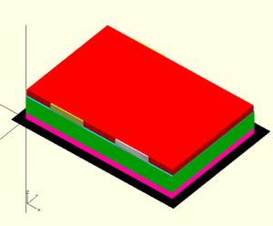
The goal of this project is to determine the viability of printing integrated circuits in passive RFID tags using pentacene, an organic semiconductor. RFID tags can be used for a wide variety of applications. The proposed application for this project is to track broomball helmets used by for intramural Broomball at Michigan Technological University. The passive RFID tags would be printed onto a glass substrate and made into a sticker for the helmets. Every time a helmet is used it can be tracked. The RFID tags can also potentially carry player information so penalty minutes, goals, assists, and other statistics can be tracked more accurately and efficiently.
Benefits/applications[edit | edit source]
- Printing RFID tags can be much cheaper than traditional manufacturing methods.[1]
- Broomball is a rough sport, and damage to the tags is inevitable. 3D printing makes tag replacement almost instantaneous (i.e. no need to continually order more and wait on shipping).
- Helmet tracking would allow the Broomball organization to predict when helmets would break, based on usage.
- A RFID system would be easy for referees and players to use, especially in cold temperatures.
RFID tag basics[edit | edit source]
RFID tags are frequently used to track the locations of items, such as materials, products, or people. There are two types of tags: passive and active. Active tags utilize an internal power source, which boosts communicability with the reader. Passive tags are powered by radio frequency (RF) energy that is transferred from the reader.[2] A passive RFID tag has been chosen for this project due to its durability and small physical footprint.
Passive tags consist of two parts: an antenna and a chip.[3] The antenna is a thin, printed pattern of a conductive material (such as copper) that serves to receive energy from the reader. The chip primarily consists of a thin-film transistor that transmits information back to the reader. It is made of five layers of material, printed on top of an amorphous substrate: a gate level (conductive metal), dielectric/insulator, surface treatment, semiconductor, and source/drain terminals.[4]
3D printing method[edit | edit source]
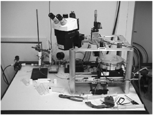
3D printing is a fast-growing field, in which solid objects are created based off of a computer model, one layer of material at a time. It allows for the reproduction of custom parts and trinkets in an easy and affordable way. Open-source printers, such as the RepRap, are continually-improving systems that are capable of reproducing themselves and are reasonably priced for home use.
RFID tags can be printed using an inkjet printer head. The organic semiconductor pentacene is not a soluble material, but a pentacene precursor may be created and mixed into solvent to form printable ink. This ink can be distributed using a standard inkjet dispenser. The ink is annealed to reform the pentacene semiconductor. A custom inkjet system can be used, requiring control software for the printer settings, usually custom made for the system or application. The inkjet system generally consists of translation stages, the inkjet dispensers, and a hot chuck for heating/annealing processes.
An example of a custom inkjet system used for this kind of application is shown in Figure 1. The inkjet system uses a piezoelectric head with nozzles allowing for a 30 µm to 60 µm variation in diameter. The solvent used to form the precursor ink solution must have a low evaporation rate, as to prevent clogging of the nozzles. The voltage settings for the inkjet should be configured to prevent satellite droplets from forming during the process.[1]
Materials[edit | edit source]
The material used in this application is pentacene, an organic semiconductor. Pentacene is a hydrocarbon consisting of five benzene rings. It has been chosen for many printed organic semiconductor applications because of its relatively high mobility, seen as high as 3 cm2/V-sec in some experiments.[1] The synthesis of pentacene will be discussed in the next section.
- Gold will be used as the gate, source, and drain material. Two nanometer diameter gold nanocrystals are the smallest crystal available from the chosen supplier. It is optimal to use the smallest crystal size available because the decreased size provides a lower the melting temperature for the source and drain contacts.[5] To condense the printed gold and evaporate the hexane solvent, the layer must be annealed. For ease of production, a low melting temperature is desireable.
- Silicon Dioxide will be used as a dielectric in the thin film transistor.
- Because pentacene is not a liquid at room temperature, a precursor must be mixed with a solvent to form the ink. The chosen precursor for this project is 13,6-N-Sulfinylacetamidopentacene.
- Anisole is the solvent to be mixed with the pentacene precursor to form the semiconductor ink.
| Material | Use/Purpose | Cost | MSDS |
|---|---|---|---|
| Gold Nanocrystal | Gate, source, drain | $50/1 mg. | MSDS |
| Silicon dioxide | Dielectric | $102/1 Kg. | MSDS |
| 13,6-N-Sulfinylacetamidopentacene
(pentacene precursor) |
Semiconductor | $262/100 mg. | MSDS |
| Anisole | Solvent | $111/1 L | MSDS |
Purity testing[edit | edit source]
] The primary method for determination of the pentacene precursor's purity is infrared spectroscopy, specifically Fourier Transform Infrared Spectroscopy (FTIR). FTIR is the process of passing infrared radiation through the precursor, at which point some radiation is transmuted and some is absorbed. A computer generates a spectrum of peaks based on how much radiation is absorbed or transmuted within the sample and back to the computer sensors. The computer performs a Fourier Transformation on the peaks in the spectrum so that the peak intensities versus the frequencies can be output and used comparatively. This spectrum is unique to every molecular structure, and a known spectrum of the pure pentacene precursor can be quantitatively and qualitatively analyzed in comparison to the sample spectrum in question to determine purity.
Quantitative analysis requires mathematically computing the intensity ratio of the pure known sample to the sample in question, and qualitative analysis can be used to simply determine if any impurities or unintended substances are present in the sample and are creating intensity peaks.[6]Elemental analysis or H NMR spectroscopy may also assist in determination of purity.[7]
While annealing the semiconductor ink to thermally convert the precursor back to pure pentacene (via a retro Diels-Alder reaction), UV-vis spectroscopy can be used to visually determine if the precursor is converting back to pentacene. A spectrum from the UV-vis can be qualitatively analyzed against the known spectrum for pentacene to determine if thermal transformation to pentacene was completed. When analyzing the final product, IR spectroscopy can again be used to qualitatively determine if pentacene is the only product left in the sample by comparing to known spectra of pure pentacene.
Synthesization and purification of semiconductor ink[edit | edit source]
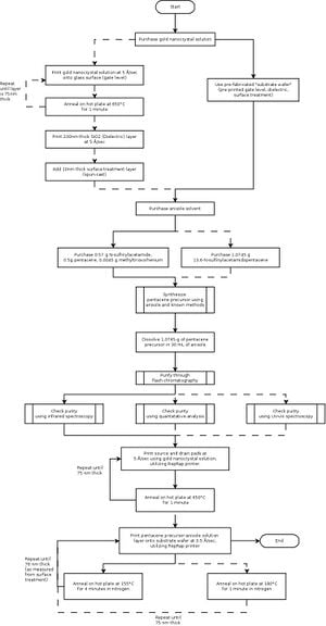
The method used to synthesizing a pentacene precursor for use as a soluble, printable semiconductor ink for this project involves the use of a Diels-Alder reaction, a reaction that allows the formation of cyclohexene rings while requiring very little energy to carry out the reaction. First, commercial pentacene must be aquired and treated with N-sulfinylacetamide. Methyltrioxorhenium is used as the reaction catalyst. The treated compound and catalyst is refluxed in a solvent for approximately two days in order to create a pentacene precursor ink solution. The compound itself, as solute, is a white microcrystalline structure that is stable in normal air conditions and is highly soluble.[8] An appropriate amount of material to use for synthesizing is 0.5 grams of pentacene, 0.57 grams of N-sulfinylacetamide, 0.0045 grams of methyltrioxorhenium, and 30 milliliters of solvent (anisole for this application).[1]The ink is purified using flash column chromatography. This method produces analytically pure samples of the precursor.
Another option for the acquisition of this ink is to purchase commercially available pentacene precursor and mix it with an appropriate solvent (such as chloroform or anisole). This product is generally designated as 13,6-N-Sulfinylacetamidopentacene, essentially the same compound described above.[9]
While the latter option is more convenient, it is preferable to synthesize the compound to reduce costs. Both methods, as well as the procedure for printing, are outlined in Figure 3.
Chip production[edit | edit source]
A RFID chip consists of five layers on top of a substrate. From bottom to top, these are: a gate level, dielectric, surface treatment, semiconductor, and source/drain. All layers except the surface treatment can easily be 3D printed (the surface treatment is spun-cast). Because of the flat, simple shape, it is possible to mass-produce pre-fabricated gate, dielectric, and surface treatment layers, which eventually saves processing time.
The steps for creating a chip are as follows:
- Identify substrate (in this case, glass)
- Print gate level, dielectric
- Spin-cast surface treatment
- Print source and drain, anneal
- Create pentacene precursor
- Purify and verify purification of precursor
- Print pentacene precursor-anisole solution
As with all operations, there are different possible procedures for each step. The differences in procedures for non-semiconductor layer production has been discussed, as has creation, purification and verification methods.
Anneal times are a large source of variance in printing. For the pentacene precursor, the optimum anneal falls between 120°C and 205°C when annealed in nitrogen..[1] By looking at saturation mobility as a function of temperature, the optimum temperature is approximately 155°C. The appropriate annealing time for this temperature is four minutes. While this is an optimal temperature, the assembly may be annealed at any temperature in the range 155-180°C, such as 180°C for one minute.[1]The order of the layers is also variable, and is dependent on function. The semiconductor layer may be either on top of or below the drain/source. In this case, the pentacene must be on top due to the difference in melting temperatures between pentacene and the gold nanocrystals. If the nanocrystals were smaller, their melting temperature would drop low enough to not overlap.
Characterization of Semiconductor Material[edit | edit source]
X-ray Diffraction[edit | edit source]
XRD can be used to analyze phases in the semiconductor material. There are generally two phases found in pentacene semiconductors. One is a single crystal phase (SCP), the other is a thin film phase (TFP). TFP is the kinetically favored phase while SCP is the more thermodynamically stable phase. Research has shown that samples with higher percentage of SCP have higher mobility than films with higher percentage of TFP. XRD could possibly be performed in situ by building or modifying an XRD machine to be used as the semiconductor is annealing on a hot plate. This way, the annealing process can be stopped as soon as the intensities reach the value required to have a higher percentage of SCP.[6]
Scanning Tunneling Microscopy[edit | edit source]
A combined scanning electron microscope (SEM) and scanning tunneling microscope (STM) can be used to perform spectroscopy on pentacene. This method allows a simultaneous characterization of morphology and surface electronic structure. SEM is used to ensure the probe of the STM is in the exact location required. STM allows you to look at electric properties in a very localized area of the sample. If STM is performed in situ, it reduces the amount that the sample is exposed to air. Air can decay the electrical properties of the semiconductor. This in situ method has been performed in vaccum conditions. To adapt for in situ analysis, the STM device can be modified to analyze the semiconductor as it is annealing to ensure required electrical properties are met.[10]
Best in class material properties[edit | edit source]
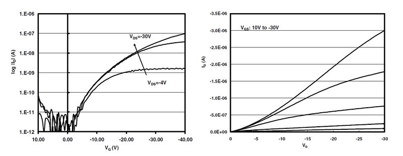
Figure 3 (below) shows best case electrical properties for pentacene semiconductors. These optimal properties were from a pentacene sample annealed at 155°C for 4 minutes. Drain and gate voltages are plotted against drain currents. As stated in the materials section, pentacene mobilities have been seen as high as 3 cm2/V-sec. However, it is more likely to see mobilities from 0.02 cm2/V-sec to 1.5 cm2/V-sec. Best case on-off ratios have been seen as high as 105.[1]
Design[edit | edit source]
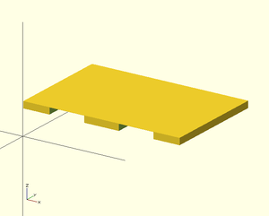
OpenSCAD is an open-source 3D CAD software that was used to model both the semiconductor layer of the RFID chip and the full chip.
OpenSCAD code for semiconductor (pentacene) layer (File:MY3701 RFID model semiconductor only.stl]):
// All dimensions are in nanometers
// Semiconductor layer (Pentacene)
difference()
{
	translate([0,10,285])
	color([1,0,0,1])
	cube([1800,1200,76]);

	translate([300,0,284])
	cube([400,1221,75]);

	translate([1100,0,284])
	cube([400,1221,75]);
}

OpenSCAD code for a full RFID chip assembly (File:MY3701 RFID model.stl]):
// All dimensions are in nanometers
// Glass base (not printed)
translate([-100,-100])
	color([0,0,0,1])
	square([2000,1440]);

// Subsequent layers are printed in order

// ...HOWEVER, Gate level+dielectric layer+surface
// treatment may be mass-produced as wafers

// Gate level (Gold)
	color([2,0,1,1])
	cube([1800,1220,75]);

// Dielectric layer (Silicon Dioxide)
	translate([0,0,75])
	color([0,1,0,1])
	cube([1800,1220,200]);

// Surface treatment
	translate([0,0,275])
	color([0,1,1,1])
	cube([1800,1220,10]);

// Source pad (Evaporated gold nanoparticles)
translate([300,0,285])
color([1,1,0,1])
cube([400,1220,75]);

// Drain pad (Evavporated gold nanoparticles)
	translate([1100,0,285])
	color([1,1,1,1])
	cube([400,1220,75]);

// Semiconductor layer (Pentacene)
difference()
{
	translate([0,10,285])
	color([1,0,0,1])
	cube([1800,1200,76]);

	translate([300,0,284])
	%cube([400,1221,75]);

	translate([1100,0,284])
	%cube([400,1221,75]);
}
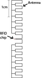
Figure 6 is a diagram of a basic RFID tag, with a compact meander-line antenna[3]
Conclusions[edit | edit source]
3D printing pentacene organic conductors is a viable way to produce integrated circuits in passive RFID tags. Research has shown that is possible to inkjet print semiconductors to form a thin film transistor for this application. Fairly good electrical properties are also possible with this method. However, there are many variables that affect the electrical performance of the semiconductor when it is printed. These variables include: anneal time, anneal temperature, phases present, and thickness of semiconductor layer. If a process can be formed where pentacene has high performing, consistent electrical properties, this method will provide a cheap alternative to traditional manufacturing methods for RFID tags.
References[edit | edit source]
- ↑ 1.0 1.1 1.2 1.3 1.4 1.5 1.6 1.7 1.8 S. Volkman et al., "Inkjetted Organic Transistors using a Novel Pentacene Precursor", University of California, Berkeley, Berkeley, California, 2003.
- ↑ Atlas RFID Solutions website, 2013.
- ↑ 3.0 3.1 S. Lam, P. Nikitin and K.V. Seshagiri Rao, "Antenna Design for UHF RFID Tags: A Review and a Practical Application", IEEE Transactions on Antennas and Propagation, Vol. 53, No. 12, 2005.
- ↑ P. Baude, D. Ender, T. Kelley, M. Hasse, D. Muyres, and S. Theiss, "Organic semiconductor RFID transponders", 3M Company, St. Paul, Minnesota, 2003.
- ↑ B. Corain and G. Schmid, "Nanoparticulated Gold: Syntheses, Structures, Electronics, and Reactivities", Wiley-VCH Verlag GmbH & Co. KGaA, 69451 Weinheim, Germany, 2003.
- ↑ 6.0 6.1 N. Singh, "DEPOSITION AND CHARACTERIZATION OF PENTACENE THIN FILMS", University of North Texas, Denton, Texas, 2003.
- ↑ Ali Afzali, Christos D. Dimitrakopoulos, Tricia L. Breen, "High-Performance, Solution-Processed Organic Thin Film Transistors from a Novel Pentacene Precursor" IBM Research Division, T.J. Watson Research Center, Yorktown Heights, NY, Rep. 10.1021/ja0266621, 2002.
- ↑ Ali Afzali, Christos D. Dimitrakopoulos, Tricia L. Breen, "High-Performance, Solution-Processed Organic Thin Film Transistors from a Novel Pentacene Precursor" IBM Research Division, T.J. Watson Research Center, Yorktown Heights, NY, Rep. 10.1021/ja0266621, 2002.
- ↑ Prof. Cherie R. Kagan (2005). Fabrication of Organic Field Effect Transistor Device Using a Soluble Pentacene Precursor [Online]. Available: http://web.archive.org/web/20161017172516/http://www.sigmaaldrich.com:80/materials-science/organic-electronics/soluble-pentacene-precursors.html
- ↑ A. Birkner et al., "STM assisted in-situ spectroscopy on nano-sized crystallites of organic semiconductors", Ruhr University, Bochum, Germany, 2004.