Gallium arsenide (GaAs) is a semiconductor material that is used in a wide variety of applications ranging from circuits to solar cells. Solar cells of GaAs can be produced using both bulk and thin film growth methods.
Material Processing[edit | edit source]
Bulk Growth[edit | edit source]
There are two common ways to produce GaAs using bulk growth, Liquid-Encapsulated Czochralski (LEC) growth, and Vertical Gradient Freeze (VGF) technology.[1]
Liquid-Encapsulated Czochralski Growth(LEC) LEC growth is accomplished by melting high-purity arsenic and gallium in a high temperature vessel, and slowly cooling to produce a single crystal. The GaAs crystal produced using this method however has some impurities such as significant levels of carbon, and numerous dislocations. These impurities cause the semiconductor to be unusable for some applications. Vertical Gradient Freeze Technology (VGF) VGF growth works by placing high purity arsenic and gallium in an enclosed quartz ampoule with a crystal of GaAs. The arsenic and gallium are melted, and then brought into contact with the GaAs crystal. When cooled slowly, a single crystal of GaAs is formed. The single crystal formed has many of the same impurities as LEC growth crystals, which restricts the utility of the crystals.
Typical dimensions of the semiconductor crystals are 1-6 inches in diameter and 2-30 inches long. The usual rate of crystal growth is 1-5mm per hour.[2]
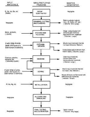
Cutting, Polishing, and Etching The bulk crystals (boule) produced are cylindrical with conical ends, thus they need to be cut, polished and etched before they can be used. During processing the conical ends are cut and wasted, the boule is ground to ensure a uniform diameter over the length, the crystals are aligned using x-ray diffraction, and the boule is cut into wafers. Just forming the correct shape results in nearly one third of the total mass being wasted. Even further processing is required to etch off the damaged layer of semiconductors from sawing and to polish the semiconductor. As a result of processing, nearly 50% of the semiconductor is wasted.[2]
Thin Film Growth[edit | edit source]
Thin films of GaAs have many advantages over large single crystals of GaAs when it comes to being used in solar cells. Thin films lack some of the impurities found in large crystals, and are capable of being used without requiring extensive slicing. The rest of the case study will be dedicated to thin film GaAs semiconductors.
The most common thin film growth methods for producing GaAs films are Metalorganic Chemical Vapour Deposition (MOCVD) and Molecular Beam Epitaxy (MBE).
Metalorganic Chemical Vapour Deposition (MOCVD)
MOCVD is a chemical vapour deposition method of depositing epitaxial films using surface reactions of organic compounds, metalorganics or metal hydrides. The growth of the epitaxial film is the result of a chemical reactions, and not physical deposition. MOCVD of GaAs requires a reaction chamber with gas injection units, a temperature control system, and a pressure control system.[3] During MOCVD of GaAs, trimethylgallium Ga(CH3)3 and arsine AsH3 are consumed.[4]
Molecular Beam Epitaxy (MBE)

MBE is the process of depositing epitaxial films on a substrate under ultrahigh vacuum (UHV) conditions using atomic or molecular beams. The atomic or molecular beams are generated from elemental feedstocks in Knudsen-type effusion cells. The beams travel in straight paths to the substrate where they condense and grow under kinetically controlled conditions.[2] During MBE, ultra pure gallium and arsenic are consumed.
Waste during Production[edit | edit source]
Preliminary Calculations[edit | edit source]
Current Production methods of GaAs semiconductors produce a large amount of waste. To determine the amount of waste produced during production of GaAs solar cells, we must first determine the amount of GaAs per Area/Wattpeak. The calculations are seen below.
GaAs per Area
Size of Panels = 10 inches x 9 inches[5]
Number of Cells per Panel = 18[5] Area of Cell = (90 in2/18)*.00064516 m2/in2 [((Area Panel)/(Number Cells))*(conversion from in.2 to m2)] Area of Cell =.0032258 m2 GaAs per Cell = 10 grams[5] GaAs per Area = 10 g /.0032258 m2 [(GaAs/Cell)/(Area Cell)]
GaAs per Area = 3100 g/m2
GaAs per Watt
Peak Power per Cell = 880mW[5] Peak Power per Area = 880mW /.0032258 m2 [(Power/Cell)/(Area Cell)] Peak Power per Area = 272.8 W/m2 GaAs per Wattpeak = 3100 g/m2 / 272.8 W/m2 [(GaAs/Area)/(Power/Area)]
GaAs per Wattpeak = 11.4 g/Wpeak
Metalorganic Chemical Vapour Deposition Waste[edit | edit source]
Using the data from the preliminary calculations, and the utilization efficiency given below for MOCVD, the Waste GaAs per Area/Wattpeak of MOCVD can be determined.
Average Material Utilization Efficiency = 30%[6]
Waste GaAs per Area
Waste GaAs per Area = (3100 g/m2/.3)-3100g/m2 [(GaAs/Area)/(Percentage Waste)-(GaAs/Area)] Waste GaAs per Area = 7233 g/m2
Waste GaAs per Wattpeak
Waste GaAs per Wattpeak = (11.4 g/Wpeak/.3)-11.4g/Wpeak [(GaAs/Wattpeak)/(Percentage Waste)-(GaAs/Wattpeak)]
Waste GaAs per Wattpeak = 26.6 g/Wpeak
Molecular Beam Epitaxy Waste[edit | edit source]
Similar to the waste rates of MOCVD, the waste rates of MBE can be determined using the preliminary calculations and the MBE utilization efficiencies. However, the waste rates for MBE are given for Ga and As individually.
Waste Ga Calculations
Material utilization efficiency for Ga = 40-70%[6]
Average Material utilization efficiency for Ga = 55%
Waste Ga per Area
Grams of Ga per Area = 3100 g/m2*69.723/(69.723+74.922) [(GaAs/Area)*(Wt% Ga)] Grams of Ga per Area = 1494.3 g/m2 Waste Ga per Area = (1494.3 g/m2/.55)-1494.3g/m2 [(Ga/Area)/(Percentage Waste)-(Ga/Area)]
Waste Ga per Area = 1222.6 g/m2
Waste Ga per Wattpeak
Grams of Ga per Wattpeak = 11.4 g/Wattpeak*69.723/(69.723+74.922) [(GaAs/Wattpeak)*(Wt% Ga)] Grams of Ga per Wattpeak = 5.495 g/Wattpeak Waste Ga per Wattpeak = (5.495 g/Wpeak/.55)-5.495g/Wpeak [(Ga/Wattpeak)/(Percentage Waste)-(Ga/Wattpeak)]
Waste Ga per Wattpeak = 4.496 g/Wpeak
Waste As Calculations
Material utilization efficiency for As = 10-20%[6] Average Material utilization efficiency for As = 15%
Waste As per Area
Grams of As per Area = 3100 g/m2*74.922/(69.723+74.922) [(GaAs/Area)*(Wt% As)] Grams of As per Area = 1605.7 g/m2 Waste As per Area = (1605.7 g/m2/.15)-1605.7g/m2 [(As/Area)/(Percentage Waste)-(As/Area)]
Waste As per Area = 9099 g/m2
Waste As per Wattpeak
Grams of As per Wattpeak = 11.4 g/Wattpeak*74.922/(69.723+74.922) [(GaAs/Wattpeak)*(Wt% As)] Grams of As per Wattpeak = 5.9 g/Wattpeak Waste As per Wattpeak = (5.9 g/Wpeak/.15)-5.9g/Wpeak [(As/Wattpeak)/(Percentage Waste)-(As/Wattpeak)]
Waste As per Wattpeak = 33.4 g/Wpeak
Recycling[edit | edit source]
Collecting Waste[edit | edit source]
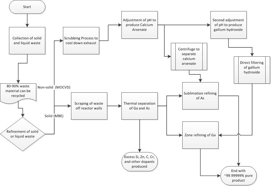
Semiconductor waste from MBE occurs mainly as a solid waste coating the reactor walls and parts, while the MOCVD process creates non solid waste in the form of exhaust vapors drawn off of the epitaxial reactors.
Solid Waste
The coating of the reactor walls and parts forms a solid waste material, which can be collected by simply scraping it off off reactor components. The solid waste material collected in this manner may be contaminated with dopants such as Si, Zn, C and Cr, as well as with GaAsP, arsenic oxides, and phosphorous oxides. These dopants however usually only have concentration levels of only 1018[2] atoms/cc.
The energy collection cost for this solid waste is assumed to be negligible, as the solid waste needs to be removed in current production processes.
Non-solid Waste
The collection of semiconductor waste from exhaust vapors is not as straight forward as the collection of solid waste material. In order to collect the waste from the exhaust, the exhaust vapors undergo a series of "scrubbing" processes, in which cooled water would be sprayed into the vapor, cooling it off until the relative temperature of the desired components in the exhaust reach a temperature where it changes from a gas to either liquid or solid phase.[7] This material would then be collected and, depending upon the contaminants (which would include the dopants used to create the thin films), would undergo multiple purification process in order to reach the desired purity for reuse.
To determine the cost of collecting non-solid waste, we need to determine the cost of operating a water scrubber. The calculations below are for removing arsenic from the exhaust, but it is assumed the same energy cost will exist for removing gallium.
Energy cost to remove 3kg As = 34,470 kJ[8]
Energy Cost = (34370 kJ *2.7778*10^-4 kw*hr/kJ) / 3000 [(Energy Cost)*(kJ to kW-hrs conversion)/(Number of grams As)]
Energy Cost =.003182 kW-hrs/g
Collection Efficiency
Since the primary methods of material loss are accounted for above, it can be assumed that, while a certain loss of materials will always occur, most of the materials will be captured and re-purified. Materials will be lost in the water scrubbing method, as not all of the waste materials will be condensed into liquid and so some reusable gases will escape into the atmosphere despite the taken precautions. The solid wastes will undoubtedly be captured entirely, with little to no loss occurring. However, when the purification process takes place, some Ga and As will undoubtedly be lost, as defects and impure materials will have to be removed from the system in order to purify the elements to their required level of purity. It can be assumed that about 80-90% of the materials will be reusable though, depending upon the standards of quality enacted in processing the waste materials.
Process of recycling and re-purification[edit | edit source]
Non-Solid Waste recycling and re-purification Before the non-solid waste produced from the MOCVD process can be recycled and re-purified, it must first be turned into solid waste.
Non-Solid Waste to Solid Waste Conversion
The waste water obtained from the water scrubbing process is adjusted to a pH between 11.5 and 12 with the use of sodium hydroxide. After the pH is correctly adjusted, a soluble calcium salt is added to the mixture. This soluble calcium salt reacts with the arsenate, and produces a calcium arsenate precipitate which can be removed using a centrifuge. After the calcium arsenate precipitate is removed the pH is readjusted to between 6 to 8 using sulfuric acid, which causes gallium hydroxide to precipitate out, which can be collected and filtered.[2]
The energy cost of converting the non-solid waste to solid waste can be estimated by determining the energy cost of the centrifuge process.
Energy cost Centrifuge = 18.5 kW-hrs[9]
Estimated Capacity = 2000 grams GaAs (Mixed into water)
Energy cost Centrifuge per gram = 18.5 kW-hrs/ 2000 grams [(Energy cost)/(Capacity)]
Energy cost Centrifuge per gram =.00925 kW-hrs/g
Purifying Gallium Hydroxide
To obtain gallium instead of the solid waste gallium hydroxide, a process of electrowinning can be performed. To perform electrowinning the gallium hydroxide is redissolved in a caustic solution, and electrodes are placed into the material. When a current passes between the electrodes, the gallium metal is deposited onto a electrode and is collected[10].
The energy cost to retrieve the gallium through electrowinning is shown below.
Energy Cost = 2 kW-hrs/kg[11]
Energy Cost =.002 kW-hrs/g
This gallium metal can be processed further using the gallium zone refinement described in the next section.
Purifying Calcium Arsenate
The calcium arsenate can be further processed using the sublimation refining process described in the next section.
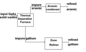
Solid Waste recycling and re-purification The recycling of GaAs solid waste can be accomplished in three steps, Thermal Separation, Sublimation Refining of Arsenic, and Gallium Zone Refinement.
Thermal Separation
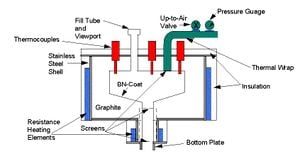
Thermal separation is the process of separating gallium and aresenic using elevated temperatures and reduced pressures. To begin separation solid GaAs waste is placed into a graphite or SiC crucible inside of a thermal separation furnace. The furnace is heated to above 1050 degrees C for 2-3 hours, and the pressure inside is reduce to less than 1 torr. At these elevated temperatures and reduced pressures, arsenic is able to be separated out as a condensable vapor, leaving a gallium-rich residue in the crucible. Due to the low melting temperature of gallium compared to other elements, the gallium-rich residue left in the crucible is composed of a liquid gallium fraction, and a slag fraction. Filtering out the slag from the gallium-rich liquid before cooling, and condensing the arsenic vapors produces fairly pure gallium and arsenic solids.
The energy cost of operating a thermal separation furnace would be the cost of heating the GaAs, and the cost of the vacuum pump maintaining a low pressure.
Energy cost of furnace =.25 (kW-hrs/hr)/pound[12]
Energy cost of furnace per gram =.25 (kW-hrs/hr)/pound * 3 hours / 453.6 grams/pound [(Energy Cost/hr)*(Number of hours run)/(Grams to pound conversion)]
Energy cost of furnace per gram =.001653 kW-hrs/g
Energy cost of vacuum =.08 kW-hrs[13]
Estimated size of batch for vacuum = 8000 grams
Energy cost of vacuum per gram =.00001 kW-hrs/g
Energy cost thermal separation per gram =.001653 kW-hrs/g +.0001 kW-hrs/g [(Energy cost vacuum/gram) + (Energy cost furnace/gram)]
Energy cost thermal separation per gram =.001663 kW-hrs/g
Sublimation Refining of Arsenic

Although thermal separation separates gallium and arsenic fairly effectively, the arsenic can still be contaminated with more volatile contaminants like carbon. To further purify, the arsenic is put through through the process of sublimation refining. During sublimation refining, the arsenic is heated slightly above 610 degrees C, the sublimation temperature of arsenic. This heating is performed in an inert gas stream such as nitrogen, and the arsenic is transferred to and recondensed in a second chamber. To obtain higher purity arsenic, this process can be accomplished multiple times. This method works because arsenic and the impurities within will differ in partial pressures and volatility.
The calculation for the energy for sublimation refining can be estimated by determining the energy cost to heat arsenic to 610 degrees C.
Energy cost of As purification =.25 (kW-hrs/hr)/pound[12]
Estimated time for purification = 2 hours.
Energy cost of As purification per gram =.25 (kW-hrs/hr)/pound * 2 hours / 453.6 grams/pound [(Energy Cost/hr)*(Number of hours run)/(Grams to pound conversion)]
Energy cost of As purification per gram =.001102 kW-hrs/g
Gallium Zone Refining
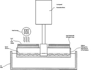
Gallium zone refining is a purification technique for gallium based upon low expectations of impurities. The process only works due to the near pure gallium obtained from thermal separation. To further purify, gallium is placed in a gallium refining pan with a spiral groove in the pan bottom, and cooled to 0 degrees C. A heat lamp is used to heat specific zones of the gallium sample, and the pan is slowly rotated. Based upon the temperature difference of solid and liquid in the sample, impurity segregation will occur, and impurities will segregate to both ends of the spiral groove in the gallium refining pan.
The energy cost associated with gallium zone refining can be estimated as the cost to spin, cool, and heat the gallium.
The energy cost for spinning will be assumed to be the same as for the centrifuge, but the capacity will be increased, as almost pure gallium is being spun.
Energy cost spinning = 18.5 kW-hrs[9]
Estimated Capacity = 20000 grams GaAs (Almost pure Gallium)
Energy cost spinning per gram = 18.5 kW-hrs/ 20000 grams [(Energy cost)/(Capacity)]
Energy cost spinning per gram =.000925 kW-hrs/g
Energy cost of refrigeration per batch is estimated as normal daily use, due to having to bring from hot to cold.
Energy cost of refrigeration = 3.1 kW-hrs[14]
Estimated Capacity = 20000 grams GaAs
Energy cost of refrigeration per gram = 3.1 kW-hrs / 20000 grams [(Energy cost)/(Capacity)]
Energy cost of refrigeration per gram =.000155 kW-hrs / gram
The energy cost of heating will be based upon furnace values used previously, however they will be quartered to account for spot heating.
Energy cost of furnace per gram =.001653 kW-hrs/g
Energy cost of heating per gram =.001653 kW-hrs/g / 4
Energy cost of heating per gram =.00041325 kW-hrs/g
Total Energy cost gallium zone refining per gram =.00041325 kW-hrs/g +.000144 kW-hrs/g +.000925 kW-hrs/g [(Cost of heating/g) + Cost of spinning/g)+(Cost of refrigeration/g)]
Total Energy cost gallium zone refining per gram =.001483 kW-hrs/g
Purity
The contamination level of Gallium and Arsenic after the above processes are completed can be as low as 5-50 ppb, or in other words the material is 99.99999% pure.[15] This purity meets the requirements for both semiconductor grade, 99.99%, and solar grade, 99.9999%.
Characterization Methods[edit | edit source]
The characterization of high purity materials is extremely difficult, and almost impossible to be adapted to in-situ methods for some materials.
The only reliable method to measure the purity of arsenic to the semiconductor and solar grade level is to react it with gallium to form GaAs crystals. Once reacted with a known gallium purity, analyzing the purity of the GaAs crystals formed can determine the purity of the arsenic used.[2]
Gallium can be more easily characterized to determine the purity level than arsenic. One of the most common methods of determining the purity of high-purity Gallium is to use Secondary Ion Mass Spectrometry (SIMS).[2] SIMS works to determine the characterization of a sample by sputtering a specimen with a primary ion beam and using a mass spectrometer to collect and analyze the secondary ions ejected from the sample. Although SIMS requires specialized equipment including a high vacuum chamber, the test could easily be performed in a small testing facility.
Downcycling[edit | edit source]
Large scale downcycling for GaAs waste currently does not exist, and will most likely not be examined in the near future. The reason that downcycling does not exist for GaAs is the limited utility of downcycled gallium and arsenic. GaAs semiconductor components account for 98% of the current gallium consumption.[16] With the narrow usage of gallium in other fields, there is no real market behind downcycling gallium. Arsenic, although more widely used in other fields than gallium, also does not have a market drive behind downcycling. Arsenic can be used to treat wood, preserve leather, kill insects, and harden lead for use in bullets, however, it is extremely toxic to humans. There is a large push to reduce the usage of arsenic in industry, especially because companies that produce arsenic products are often responsible for the environmental clean up.[2]
Producing a Recycling Plant[edit | edit source]
Part of the goal of this case study is to determine the technical viability of recycling GaAs. This can be accomplished by designing a Semiconductor Recycling Plant capable of supporting a 1 GW thin-film solar photovoltaic manufacturing facility.
Due to the high purity of our recycled material (~99.99999%) the transition between the recycling plant and the photovoltaic manufacturing facility would be rather seamless. Our proposed product meets any requirements for semiconductor and solar cell grade purity requiring zero extra steps in the process. Ideally there would be a solar photovoltaic manufacturing facility in close proximity to reduce shipping costs for both parties. The only manufacturing difficulty that may arise with our proposed process would be trying to minimize the amount of waste exhaust that is released into the atmosphere during the MOCVD process. Even if we were unable to reduce the amount of exhaust (reduce it to less than the current amount after the MOCVD process)the concentration and amount of gas is so little it would cause very little environmental concern.
Plant Capacity[edit | edit source]
Using the material waste values produced through various methods of GaAs thin-film production, we can determine the necessary capacity of a feasible recycling plant.
Supporting a MOCVD plant
The amount of material per Watt Peak wasted using MOCVD was determined to be 26.6 g/Wpeak. Using this value, and the size of the supported manufacturing plant, we can determine the daily required capacity of a recycling plant.
Required Recycling Capacity = (26.6 g/Wpeak *1 GW)/(1000 *365)[((Waste/Wpeak)*(Plant capacity))/((Gram to Kilogram conversion)*(Days/Year)]
Required Recycling Capacity = 72876.7 kg/day
Due to the separate processes that arsenic and gallium must go through, a capacity for each should be calculated. It is assumed that a 1:1 mole ratio exist for MOCVD waste.
Required Recycling Capacity As = 72876.7 kg/day *74.922/(69.723+74.922) [(Total Capacity)*(Wt% As)]144.645
Required Recycling Capacity As =37748.1 kg/day
Required Recycling Capacity Ga = 72876.7 kg/day *69.723/(69.723+74.922) [(Total Capacity)*(Wt% Ga)]
Required Recycling Capacity Ga = 35128.6 kg/day
Supporting a MBE plant
The amount of material per Watt Peak wasted using MBE was determined to be 4.496 g/Wpeak for Ga and 33.4 g/Wpeak for As. Using these values, and the size of the supported manufacturing plant, we can determine the daily required capacity of a recycling plant.
Required Ga Recycling Capacity = (4.496 g/Wpeak *1 GW)/(1000 *365)[((Waste/Wpeak)*(Plant capacity))/((Gram to Kilogram conversion)*(Days/Year)]
Required Ga Recycling Capacity = 12318 kg/day
Required As Recycling Capacity = (33.4 g/Wpeak *1 GW)/(1000 *365)[((Waste/Wpeak)*(Plant capacity))/((Gram to Kilogram conversion)*(Days/Year)]
Required As Recycling Capacity = 91506.8 kg/day
Equipment Requirements[edit | edit source]
Depending upon the solar production technique supported, the equipment requirements will vary slightly for recycling.
Supporting a MOCVD plant
The following equipment is necessary to recycle waste from a MOCVD plant.
- Water Scrubber
- Reaction chamber with Centrifuge
- Arsenic Sublimation Refiner
- Gallium Electrolyzing Unit
- Gallium Zone Refiner
Supporting a MBE plant
The following equipment is necessary to recycle waste from a MBE plant.
- Thermal Separation Furnace
- Arsenic Sublimation Refiner
- Gallium Zone Refiner
Energy for As separation and purification: 91506.8(kg/day) --> 3.81278*10^6(g/hr) (3.81278*10^6(g/hr))/(33.4(g/W))=114155 (W/hr) --> 114.155kW/hr - As to support an MBE plant. 114.155(kW/hr)*0.001102(kw-hr/g)*91506.8(kg/day)=11511.6(kW/day)
Energy required for Ga zone refining: 12318(kg/day) --> 513250(g/hr) 513250(g/hr)/4.496(g/W)=114157(W/hr) --> 114.157(kW/hr) - Ga to support MBE plant 114.157(kW/hr)*0.001483(kw-hr/g)*12318(kg/day)=2085.37(kW/day)
Total energy required: 11511.6(kW/day)+2085.37(kW/day)=13596.97kW/day
Material Flow Chart[edit | edit source]
Safety[edit | edit source]
MSDS File for Trimethylgallium
The manufacturing of semiconductors using gallium and arsenic does result in the handling of hazardous chemicals and needing to dispose of them. These waste materials can come on solid and liquid form posing many issues of containment and disposal.[6] Many PV manufacturers have a system for the management, handling, and disposal of the hazardous waste. Examples of these are secondary enclosures, ventilation systems, chemical detection, and neutralization systems, and automating delivery and process systems as much as possible.[6] The administration also deals with implementing employee training programs, and ensuring that proper emergency procedures are in place. Remotely operated cylinder valves have helped remove workers from possible contact with hazards by allowing them to operate cylinders from a distance, and also allowing them to shutdown remotely in case of an emergency.[6] Redundancy is also implemented in the critical systems that control pumps, flow regulators, valves, exhaust pumps, and any other equipment that could be critical in a spill prevention or hazard detection.
MBE and MOCVD do have their dangers but the above precautions should produce a safe working environment.
References[edit | edit source]
- ↑ R.L. Adams, Growth of high purity GaAs using low-pressure vapour-phase epitaxy, Nuclear Instruments and Methods in Physics Research Section A: Accelerators, Spectrometers, Detectors and Associated Equipment, Volume 395, Issue 1, 1 August 1997, Pages 125-128, ISSN 0168-9002, 10.1016/S0168-9002(97)00624-4. (http://www.sciencedirect.com/science/article/pii/S0168900297006244) Keywords: Low-pressure vapour-phase epitaxy; LPVPE; GaAs
- ↑ 2.0 2.1 2.2 2.3 2.4 2.5 2.6 2.7 Swartzbaugh Joseph, Sturgill Jeffery. Reduction of Arsenic Wastes in the Semiconductor Industry, 1998 (http://web.archive.org/web/20110602052056/http://www.epa.gov/nrmrl/pubs/600r02089/600R02089.pdf)
- ↑ http://en.wikipedia.org/wiki/Metalorganic_vapour_phase_epitaxy
- ↑ http://en.wikipedia.org/wiki/Gallium_arsenide
- ↑ 5.0 5.1 5.2 5.3 GaAs Solar Panel; Product Data Sheet; 3554 Chain Bridge Road, Suite 103, Fairfax, VA 22030, http://www.spacequest.com/products/SP-X.pdf, (accessed September 2011).
- ↑ 6.0 6.1 6.2 6.3 6.4 6.5 V.M. Fthenakis, B. Bowerman, Environmental Health and Safety (EHS) Issues in III-V Solar Cell Manufacturing, National PV EHS Assistance Center (http://www.bnl.gov/pv/files/pdf/art_168.pdf)
- ↑ Potter, G. U.S. Patent 4,008,056, 1977 (http://patft.uspto.gov/netacgi/nph-Parser?Sect2=PTO1&Sect2=HITOFF&p=1&u=%2Fnetahtml%2FPTO%2Fsearch-bool.html&r=1&f=G&l=50&d=PALL&RefSrch=yes&Query=PN%2F4008056)
- ↑ van Geelen, A.; Bink, P.H.M.; Giling, L.J.;, "MOCVD waste gas treatment," Photovoltaic Specialists Conference, 1993., Conference Record of the Twenty Third IEEE, vol., no., pp.717-722, 10-14 May 1993 doi: 10.1109/PVSC.1993.347002 URL: http://ieeexplore.ieee.org/stamp/stamp.jsp?tp=&arnumber=347002&isnumber=8044
- ↑ 9.0 9.1 http://web.archive.org/web/20090803213934/http://www.uscentrifuge.com:80/decanter-test-module.htm
- ↑ Recycling-Metals. Web. 9 Oct. 2011. <http://minerals.usgs.gov/minerals/pubs/commodity/recycle/recycmyb02r.pdf>.
- ↑ Electrochemistry Encyclopedia, http://web.archive.org/web/20132219143700/http://electrochem.cwru.edu/encycl/art-m02-metals.htm
- ↑ 12.0 12.1 https://web.archive.org/web/20151029022533/http://www.theschaefergroup.com:80/cruciblepot.htm
- ↑ http://www.combinedfluidproducts.com/pdfs/Operating_cost_analysis.pdf
- ↑ http://web.archive.org/web/20101231202818/http://www.fypower.org/ind/tools/products_results.html?id=100210
- ↑ Bautista, R. G. 2003. Processing to Obtain High-Purity Gallium. JOM., 55: 23–26.(http://atmsp.whut.edu.cn/resource/pdf/1994.pdf)
- ↑ Deborah A. Kramer, Gallium, Mineral Resources Program USGS (https://minerals.usgs.gov/minerals/pubs/commodity/gallium/460303.pdf)
