Project Proposal
To create a full model of a 3-D printable piezoresistive sensor in order to detect the amount of impact that an athlete receives during a collision to monitor the possibility of a concussion.
With professional sporting leagues such as the National Football League (NFL) and National Hockey League (NHL) adding an emphasis on player safety, especially with head injuries, it is important to have a quick and reliable way to determine the amount of force a helmet receives during a collision. This information can help determine if the player sustained a concussion and if they should be taken out of the game to protect themselves. The data that is gathered throughout games can also be accumulated and help to try and make rules that help determine if new rules are necessary to protect players in the future.
The typical acceleration that is required to sustain a concussion is about 95 g-forces [1]. Which is substantially lower than the average football player receives during a hit, with a value of 103 g-forces. Luckily most of the force of the hit can be spread around most of the body, but when the large majority of the force is directed at the head, it is necessary to make sure the players who got hit have experienced a safe amount of force to head. This is why a sensor to monitor the impact would be a great idea to improve the health and safety of the players.
Project goals
- Create your team project page and add the template {{MY3701}}
- A brief description of your semiconductor material with a link to the manufacturer(s) or suppliers of it if it exists on the market.
- A description of how it could be 3D printed (e.g. compare properties like viscosity or melting temperature to existing known printable material)
- A detailed BOM of the chemicals used to make it with links to sources and prices in a table - and total cost.
- Links to MSDSs for each of the chemicals.
- A detailed description of the steps, equipment and amounts of chemicals needed to synthesize the semiconductor ink with references to sources (e.g. recipe)
- Create a diagram in Dia outlining your workflow to summarize the steps, and the equipment, processes, chemicals, steps involved. Show alternate paths and discuss the optimal route and the metrics for choosing it. Post image on project page and email Dr. Pearce your Dia file.
- Outline purification methods and the methods needed to obtain acceptable purity for your material.
- A description of the testing procedures, equipment and specifications for the equipment used to determine if you obtained your target compound.
- A list of best in class material properties for your ink.
- Discuss the characterization methods and how they could be adapted for in-situ analysis.
- List and describe applications of this semiconductor if it is printed.
- Make a basic diagram for an electronic device that could use this semiconductor and post diagram in your project page.
- Design the semiconductor portion of the device in OpenSCAD, paste the code directly into your project page
- Post the STL of your design and a link to the STL on your project page.
Literature and Product Research
The use of Polyvinylidene Fluoride (PVDF) as a material for pressure sensitive piezoresistive equipment has become a popular choice in the bio-medical research industry. A popular application found for Polyvinylidene Fluoride pressure sensitive films is to create a pressure sensitive 'Smart Catheter'[2]
Another use of pressure sensitive PVDF sensors were found for the use of heartbeat monitor[3], which is similar to the semiconductor layout we will use for our own project.
Understanding The Market
Polyvinylidene Fluoride (or PVDF) Piezoresistive Sensors are a popular choice in the field of polymer based Piezoelectric semiconductors. They are used and other applications in which the detection of impacts beyond a specific threshold may be detrimental to the integrity of the product. Although PVDF film sensors were found in many biomedical research applications (heart monitors, catheters, etc.) There were no found markets in which they are currently being sold to the public. However, other pressure sensitive adhesive strips using silicon as a base material were found for retail over the internet, with the most common being a basic deformation-sensitive adhesive strip. The price found for a basic version of this product was $7.50[4], with everything included, except the circuitry to detect the current variations caused from impact or deformation. With this price, it seems very viable to implement several of these sensors within helmets, especially with the high cost lawsuits being passed over head to head collisions. It is believed that the polymer version of these sensors will have the possibility to be competitive with the Si-based sensor price range, as listed in the B.O.M. in the Materials section of the page.
Design
Due to the Piezoelectric nature of PVDF once polarized, the design of a pressure sensor using this material is fairly simple. The process of manufacturing the flowchart can be seen below:
(*Insert DIA Manufacturing process Flowchart Here*)
The creation of a circuit to allow this piezo-resistive material to successfully be monitored and recorded can be seen below; (This excludes the computer software capable of compiling the data for analysis)
-
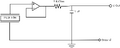
Figure 2: Elementary circuit design for PVDF pressure sensor
The circuit uses one resistor, one voltage amplifier, one capacitor, all linked around a PVFD film and excited with a power source of two 3 Volt batteries. The circuitry concept was inspired by the layout used for the heartbeat monitor source, and was re created using Dia.
- From the below dimensions used in OpenSCAD, the capacitance of the 25 micron thick PVDF layer can be determined using the following equation:

with epsilon being permittivity: relative(12 for PVDF)*space()

A = active area of film electrodes = 32mm x 13mm
t = film thickness = 25um
with a resulting PVDF film capacitance of:

A 3-D model of the project was created on OpenSCAD to give a visual representation of the final product. Below is the OpenSCAD code (in mm) and STL Link:
cube([23,19,1]);
translate([27,0,0])cube([23,19,1]);
color([0,0,1])translate([9,3,1]) cube([32,13,.025]);
color([0,1,1])translate([0,0,1.025]) cube([23,19,3]);
color([0,1,1])translate([27,0,1.025]) cube([23,19,3]);
color([0,1,1])translate([23,0,1.025]) cube([4,2,0.5]);
color([0,1,1])translate([23,17,1.025]) cube([4,2,0.5]);
-

Figure 3: OpenSCAD .stl file of piezo-resistive impact sensor
Materials
There are four main materials that will be used to create the sensor, they are: Polyvinylidene fluoride (PVDF), Mylar (which is the brand name of polyethylene terephthalate), Polydimethylsiloxane (PDMS) and silver paste. PVDF is the material that is used as the semiconductor and is highly piezoelectric[6] making it a very desirable material to be used for pressure sensor applications. It has a melting temperature of 160oC[7] PVDF is compared below to some other commonly used 3D printing inks. These inks all use the extrusion deposition technique, which is the most common technique used for reprap 3D printers. The material is wound around a coil and then heated up and melts. It is then sent through a nozzle and the material is then deposited layer by layer in both the vertical and horizontal directions creating the part that is desired.
Silver paste was chosen as the metal electrode because of its capabilities to stand up to high voltages and continue to work with voltage spikes[8]. The capabilities to work through voltage spikes will be important since there will be numerous incidents within a single game where the player will experience some force in the head.
| Material | Melting Temperature (oC) |
|---|---|
| Polyvinylidene Flouride | 160 |
| Polycarbonate (PC)[9] | 155 |
| Polylactic Acid [10] | 150-160 |
| Polyethylene terephthalate (PET)[11] | 250-260 |
The complete list of materials that are required in order to make the sensor is shown below, along with links to the MSDS pages for each of the materials and bulk material pricing.
| Material | Health | Fire | Reactivity | Personal Protection | Cost |
|---|---|---|---|---|---|
| PVDF MSDS[12] | 0 | 1 | 0 | A | $208.00per 100g[13] |
| Mylar MSDS[14] | 1 | 1 | 0 | $1.69 per 100g[15] | |
| PDMS MSDS[16] | 2 | 1 | 0 | J | $48.4 per 100mL[17] |
| Silver Paste MSDS[18] | 2 | 1 | 0 | $172.00 per 25g[19] |
Cost
| Material | Cost per part ($) |
|---|---|
| Polyvinylidene Flouride | $0.39 |
| Mylar | $0.04 |
| PDMS | $1.22 |
| Silver Paste | $3.21 |
| Total | $4.86 |
Semiconductor Synthesis
Thin film PVDF of thickness under 100 microns will form the pizeo-electric beta phase of the polymer versus the non pizeo-electric alpha phase. These thin film PVDF semiconductors therefore do not require to be stretched or annealed to display pizeo-electric properties. Since the PVDF layer in the proposed assembly is 25 microns it is predicted to form the beta phase after 3D printing do to residual stresses.
3D Printing Process
The following outlines a 3D printing process of piezo-resistive semiconductors using Polyvinylidene Flouride (PVDF) as the semi-conductive material, Mylar (Biaxially-oriented polyethylene terephthalate) as a barrier material for human skin contact, and Polydimethylsiloxane (PDMS) as a corrosion resistant and strain inducing layer using a RepRap 3D printer.
Steps:
- First acquire all bulk materials.
- Then the purchased PDMS liquid must be mixed with a cross linking agent, such as methyltrichlorosilane, to produce a material in the solid state. [1][20]
- Then all bulk solid PDMS, PVDF, and Mylar will be ground and extruded into a size usable by the RepRap printer.
- After extrusion preperation of the RepRap printer for easy removale of printed parts will be done.
- Cleaning of the printer bed with acetone and/or methanol will be conducted in an attempt to remove all unwanted organic solids. This step will be subsequently done after printing of all different assembly layers.
- The Mylar layer will be printed first using a extrusion nozzle temperature greater then 260 degrees C.
- Next the PVDF layer will be printed using an extrusion nozzle temperature greater then 160 degrees C.
- Using silver paste conductive traces can be printed onto the PVDF layer for use in the signal circuit.
- Finally the PDMS layer will be printed, in this layer extrusion nozzle temperature will need to be adjusted until the PDMS become sufficiently printable.
- After all layers are printed and the part completed the PVDF layer will be contact poled using a electric field of 30MV/m or above to enhance the pizeo-electric effect.
Considerations for 3D Printing
Current iterations of the RepRap 3D printing project can not print layers of objects at resolution less then 50 microns.[2][21] Therefore for this semiconductor projct to be produced using the RepRap printer the technology or process for printing layers with resolutions of 25 microns or less would have to be developed.
Dia Flowchart Diagram

Semiconductor Assembly Testing
In-situ analysis of the semiconductor is limited to measuring the electrical resistance of the PVDF layer after the silver paste contacts have been printed onto it and then again after it has undergone the poling process. Electrical resistance will be greater after contact poling of the material if poling was sufficient.[3][22]
Discussion
Using the information found during the literature search, and applying it to the concept of a viable, 3-D printable piezo-resistive impact monitoring system for sport helmet applications, the following could be deduced from the allotted time frame for research and development:
- 3-D printing of a PVDF Piezo-resistive impact sensor is highly viable, with all materials being polymers with melting points within the 3-D printer's capabilities. (Silver ink being the only exception of not being a polymer)
- In the application of a high impact environment (such as contact sports) compared to the model's original purpose of a heartbeat monitor[23], a change in PVDF strip dimensions (as well as a lesser sensitive, high amplitude range circuit) may be needed to avoid catastrophic failure and false readout noise during use.
- In addition, a correlation of work function[24] (Phi) in relation to strain directed in the "3" direction (direct bending, puncture shear, "z" direction for flat x-y oriented strip) will be needed for the specific condition of the PVDF film (polarization, capacitance, voltage output) in order to accurately monitor the intensity level necessary for high impact collisions (and ranking their severity).
- Due to the rough detection area of the impact sensing part (32mm x 13mm), the effect of impacts occurring on regions away from the sensor, and the effect it has on impact accuracy, still requires further research and field study to accommodate those forces.
- That being said, the idea of applying several monitors per helmet (5, one on all four sides, with one on top crown) could be a more accurate layout to detect impacts at their source. With the cost effectiveness of $4.86 per part prior to circuitry, implementing 5 sensors would keep the cost below $25 dollars per helmet less circuitry.
Conclusion
Although all of the aspects for creating an accurate PVDF, Piezo-resistive, impact monitoring sensor with circuitry for helmets and other impact applications have not been fully explored during the duration of this research, I feel it is a very viable, cost effective, 3-D printable concept which could be created and applied to impact sports for concussion monitoring, and other impact sensitive applications in the future.
Resources
- ↑ http://www.sciencedaily.com/releases/2010/06/100624092526.htm
- ↑ Tushar Sharmaa, Sang-Soo Jea, Brijesh Gillb, John X.J. Zhanga, (2012), Patterning piezoelectric thin film PVDF–TrFE based pressure sensor for catheter application, http://www.sciencedirect.com/science/article/pii/S0924424711005012
- ↑ Yi-Yuan Chiua, 1, Wan-Ying Linb, 1, Hsin-Yao Wangb, Song-Bin Huanga, Min-Hsien Wua, (2013), Development of a piezoelectric polyvinylidene fluoride (PVDF) polymer-based sensor patch for simultaneous heartbeat and respiration monitoring, http://www.sciencedirect.com/science/article/pii/S0924424712006310
- ↑ http://www.seeedstudio.com/depot/piezo-sensor-ldt1028k-lead-attachments-p-687.html?cPath=84_88&zenid=020999c566d2f31841dc54602b7d02ef
- ↑ Measurement Specialties, Inc. (1999), Piezo Film Sensors Technical Manual, http://resenv.media.mit.edu/classes/MAS836/Readings/MSI-techman.pdf source
- ↑ "PVDF." http://en.wikipedia.org/wiki/Polyvinylidene_fluoride.
- ↑ "PVDF Properties." http://www.polymerprocessing.com/polymers/PVDF.html
- ↑ "Piezo Film Sensors Technical Manual" pg 13 http://resenv.media.mit.edu/classes/MAS836/Readings/MSI-techman.pdf
- ↑ "Polycarbonate." http://en.wikipedia.org/wiki/Polycarbonate
- ↑ "Polyactic Acid" http://en.wikipedia.org/wiki/Polylactic_acid
- ↑ "Polyethylene terephthalate" http://en.wikipedia.org/wiki/Polyethylene_terephthalate
- ↑ "PVDF MSDS." dotmar.com.au. N.p., n.d. Web. 12 Oct. 2013. <http://www.dotmar.com.au/images/stories/pdfs/symalit_pvdf.pdf>.
- ↑ "Polyvinylidenefluoride - Granule ." www.goodfellow.com. N.p., n.d. Web. 12 Oct. 2013. <http://www.goodfellow.com/catalogue/GFCat4I.php?ewd_token=xS9p6K0dbfBNkirTPct21RMqoC2Tg0&n=Ez90cHNg4TJ3PIQNCnXKlGI7kUSCOG>.
- ↑ "PVDF MSDS." dupont.com N.p., n.d. Web. 12 Oct. 2013. <http://msds.dupont.com/msds/pdfs/EN/PEN_09004a2f8002e2ee.pdf>.
- ↑ www.amazon.com. N.p., n.d. Web. 12 Oct. 2013. <http://www.amazon.com/CAP-mil-Mylar-Reflective-Film/dp/B0001WW40Q>.
- ↑ "PDMS MSDS." www.sciencelab.com N.p., n.d. Web. 12 Oct. 2013. <http://www.sciencelab.com/msds.php?msdsId=9924928>.
- ↑ www.amapolymer.com. N.p., n.d. Web. 12 Oct. 2013. <http://www.ampolymer.com/Standards/PDS.html>.
- ↑ "Silver Paste MSDS." www.sciencelab.com N.p., n.d. Web. 13 Oct. 2013. <http://www.sigmaaldrich.com/MSDS/MSDS/DisplayMSDSPage.do?country=US&language=en&productNumber=735825&brand=ALDRICH&PageToGoToURL=http%3A%2F%2Fwww.sigmaaldrich.com%2Fcatalog%2Fproduct%2Faldrich%2F735825%3Flang%3Den>.
- ↑ www.sigmaaldrich.com. N.p., n.d. Web. 13 Oct. 2013. <http://www.sigmaaldrich.com/catalog/product/aldrich/735825?lang=en®ion=US>.
- ↑ BYU PDMS N.p., n.d. Web. 16 Oct. 2013. <http://www.photonics.byu.edu/PDMS.phtml>.
- ↑ Micron Printing Web. 16 Oct. 2013. <http://forums.reprap.org/read.php?279,186168,186168>.
- ↑ Review of In-situ Fabrication Methods of Piezoelectric Wafer Active Sensor for Sensing and Actuation Applications Web. 16 Oct. 2013. <http://www.me.sc.edu/research/lamss/pdf/conferences/c111_spie2005_5765-04.pdf>.
- ↑ Yi-Yuan Chiua, 1, Wan-Ying Linb, 1, Hsin-Yao Wangb, Song-Bin Huanga, Min-Hsien Wua, (2013), Development of a piezoelectric polyvinylidene fluoride (PVDF) polymer-based sensor patch for simultaneous heartbeat and respiration monitoring, http://www.sciencedirect.com/science/article/pii/S0924424712006310
- ↑ http://en.wikipedia.org/wiki/Work_function
Contact Info
Chris Shaw - Email: cjshaw@mtu.edu
Alex Seidl - Email: ajseidl@mtu.edu
Kyle Myszka - Email: kemyszka@mtu.edu