No edit summary |
No edit summary |
||
| (One intermediate revision by the same user not shown) | |||
| Line 12: | Line 12: | ||
=='''Biography'''== | =='''Biography'''== | ||
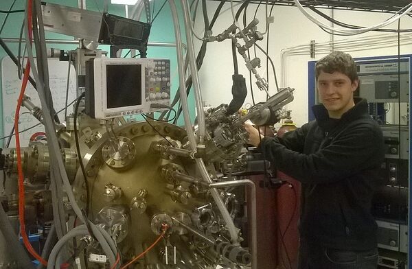
Craig is a fourth-year materials science and engineering student at Michigan Technological University with a background in R&D and product development in the polymer and semiconductor industries. He is currently engaged in research on Al additive manufacturing through the [http://www.appropedia.org/Category:MOST Pearce Research Group at Michigan Tech in Open Sustainability Technology (MOST)]. Past work with MOST includes molecular beam epitaxy (MBE) of thin films for integrating III-V semiconductors on Si substrates, and characterization of zinc oxide nano-powders. | |||
=='''Research Interests'''== | =='''Research Interests'''== | ||
* | * Photovoltaics | ||
* | * Additive Manufacturing | ||
*Nanotechnology | * Nanotechnology | ||
=='''Engineering Experience'''== | |||
==='''Product Development, Bemis Company (Jan 2016 – July 2016)'''=== | |||
#Implemented design of experiments (DOE) methodology to support product development of flexible packaging with wider ultrasonic welding window | |||
#Developed novel microscopy characterization method to understand failure mechanisms of films during ultrasonic welding process, leading to a technical solution | |||
==''' | ==='''Research and Development, Bemis Company (Jul 2016 – Dec 2016, May 2017 – Aug 2017)'''=== | ||
*Technology transfer of two technology platforms from research and pilot scales to manufacturing scale | |||
*Developed communication skills with manufacturing facility engineers and operators through commercial and pilot scale manufacturing trials | |||
*Experience in polymer compounding, blown film and cast extrusion, coating/printing | |||
===''' | ==='''Research and Development, Hemlock Semiconductor (May 2018 – Aug 2018)'''=== | ||
*Optimization of single-crystal Si solidification to reduce dislocation densities | |||
*Failure analysis with optical and electron microscopy, XRD, and XRF | |||
*Initiated manufacturing engineer/operator discussion resulting in waste savings | |||
=='''Research Experience'''== | |||
===''' | ==='''Integrating III-V Semiconductors on Si Substrates (Aug 2014 – Dec 2015)'''=== | ||
*Molecular beam epitaxy (MBE) growth of thin film semiconductors, metals, and oxides, with focus of integrating III-V thin films on silicon substrates for high-efficiency solar cells | |||
==='''Arc welding additive manufacturing of Al-Sc alloys (Sep 2018 – Present)'''=== | |||
*Al-Sc alloy development for high-strength components made through wire arc additive manufacturing (WAAM) | |||
*Manufacturing of alloy into wires (billet casting, Al extrusion, wire drawing, 3-D arc weld printing) | |||
==''' | =='''Publications'''== | ||
Abinaya, C., et al. "Structural and optical characterization and efficacy of hydrothermal synthesized Cu and Ag doped zinc oxide nanoplate bactericides." Materials Chemistry and Physics 184 (2016): 172-182. [https://doi.org/10.1016/j.matchemphys.2016.09.039] | |||
Abinaya, C., et al. "Inhibition of growth of S. epidermidis by hydrothermally synthesized ZnO nanoplates." Materials Research Express 4.7 (2017): 075401. [https://doi.org/10.1088/2053-1591/aa796d] | |||
Abinaya, Chandrasekaran, et al. "Synthetic Method Dependent Physicochemical Properties and Electrochemical Performance of Ni‐Doped ZnO." ChemistrySelect 2.28 (2017): 9014-9023. [https://doi.org/10.1002/slct.201701584] | |||
Revision as of 20:41, 22 November 2018
| Craig Ekstrum |
|---|
 |
Template:Userboxtop Template:User MOST Template:Userboxbottom
Biography
Craig is a fourth-year materials science and engineering student at Michigan Technological University with a background in R&D and product development in the polymer and semiconductor industries. He is currently engaged in research on Al additive manufacturing through the Pearce Research Group at Michigan Tech in Open Sustainability Technology (MOST). Past work with MOST includes molecular beam epitaxy (MBE) of thin films for integrating III-V semiconductors on Si substrates, and characterization of zinc oxide nano-powders.
Research Interests
- Photovoltaics
- Additive Manufacturing
- Nanotechnology
Engineering Experience
Product Development, Bemis Company (Jan 2016 – July 2016)
- Implemented design of experiments (DOE) methodology to support product development of flexible packaging with wider ultrasonic welding window
- Developed novel microscopy characterization method to understand failure mechanisms of films during ultrasonic welding process, leading to a technical solution
Research and Development, Bemis Company (Jul 2016 – Dec 2016, May 2017 – Aug 2017)
- Technology transfer of two technology platforms from research and pilot scales to manufacturing scale
- Developed communication skills with manufacturing facility engineers and operators through commercial and pilot scale manufacturing trials
- Experience in polymer compounding, blown film and cast extrusion, coating/printing
Research and Development, Hemlock Semiconductor (May 2018 – Aug 2018)
- Optimization of single-crystal Si solidification to reduce dislocation densities
- Failure analysis with optical and electron microscopy, XRD, and XRF
- Initiated manufacturing engineer/operator discussion resulting in waste savings
Research Experience
Integrating III-V Semiconductors on Si Substrates (Aug 2014 – Dec 2015)
- Molecular beam epitaxy (MBE) growth of thin film semiconductors, metals, and oxides, with focus of integrating III-V thin films on silicon substrates for high-efficiency solar cells
Arc welding additive manufacturing of Al-Sc alloys (Sep 2018 – Present)
- Al-Sc alloy development for high-strength components made through wire arc additive manufacturing (WAAM)
- Manufacturing of alloy into wires (billet casting, Al extrusion, wire drawing, 3-D arc weld printing)
Publications
Abinaya, C., et al. "Structural and optical characterization and efficacy of hydrothermal synthesized Cu and Ag doped zinc oxide nanoplate bactericides." Materials Chemistry and Physics 184 (2016): 172-182. [1]
Abinaya, C., et al. "Inhibition of growth of S. epidermidis by hydrothermally synthesized ZnO nanoplates." Materials Research Express 4.7 (2017): 075401. [2]
Abinaya, Chandrasekaran, et al. "Synthetic Method Dependent Physicochemical Properties and Electrochemical Performance of Ni‐Doped ZnO." ChemistrySelect 2.28 (2017): 9014-9023. [3]