Solar Cells are devices that convert solar energy (incident photons) into electricity. So far, Silicon is the mostly used material in the solar cell industry, because of its cost, availability and the presence of appropriate manufacturing technology. However, the problem with Silicon is its indirect bandgap (1.12 eV). Apart from Silicon, III-V and II-VI compounds have got enormous potential for solar cell applications because many of them have direct, optimum optical bandgap, along with high optical absorption capability. On top of this, structural, electrical and optical properties can be optimized towards higher efficiency while using ternary and quaternary III-V compounds. Typically, III-V and II-VI solar cells yield higher efficiency than Silicon. However, these solar cells involve higher fabrication cost, and, sometimes require modified fabrication technology.
The solar cell market[edit | edit source]
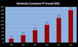
Solar cell industry is a fast growing market. The Compound Annual Growth Rate (CAGR) of Photovolaic Cell installations was 44% between 2000 and 2014. In terms of PV module production in 2014, China and Taiwan hold the lead position with a total share of 69%. Europe contributed with a share of 6%. Japan, USA and Canada- each contributed 4% of the production. There was about 184 GW of cumulative PV solar installed in the world at the end of 2014. By 2012, the 100 GW milestone was passed. The 200 GW milestone will most likely be passed in 2015.<ref>http://solarcellcentral.com/markets_page.html<ref>The installed PV base is roughly 20% residential rooftops, 20% commercial buildings like hotels and malls, and 60% utility plants connected to the grid. In 2014, Germany accounted for about 21% (38 GWp) of the cumulative PV capacity installed worldwide. PV covered almost 7% of Germany's electricity demand in 2014, avoiding around 25 Million Ton CO2 emissions.<ref>https://www.ise.fraunhofer.de/de/downloads/pdf-files/aktuelles/photovoltaics-report-in-englischer-sprache.pdf<ref>== My goal ==
I think, for making a useful trade-off between cost and efficiency, fabricating hybrid III-V solar cells (with Si or organic materials) is the most viable option. So, this is the area I want to focus on in the future. The major challenge here will always be to find the appropriate low-cost fabrication technology for making hybrid cells with minimum defects and reasonable lifetime. Quantum dots can also revolutionize the current solar cell industry. My goal is to investigate materials and to develop technologies for the mass production of high-efficiency, low-cost solar cells.
My works[edit | edit source]
An investigation into III–V compounds to reach 20% efficiency with minimum cell thickness in ultrathin-film solar cells[edit | edit source]
Authors: K A S M Ehteshamul Haque (Me), Md. Mehedi Hassan Galib
Journal of Electronic Materials, vol. 42, no. 10, pp 2867-2875. DOI: 10.1007/s11664-013-2693-x
Link: http://link.springer.com/article/10.1007%2Fs11664-013-2693-x
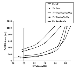
Abstract: III–V single-junction solar cells have already achieved very high efficiency levels. However, their use in terrestrial applications is limited by the high fabrication cost. High-efficiency, ultrathin-film solar cells can effectively solve this problem, as their material requirement is minimum. This work presents a comparison among several III–V compounds that have high optical absorption capability as well as optimum bandgap (around 1.4 eV) for use as solar cell absorbers. The aim is to observe and compare the ability of these materials to reach a target efficiency level of 20% with minimum possible cell thickness. The solar cell considered has an n-type ZnSe window layer, an n-type Al0.1Ga0.9As emitter layer, and a p-type Ga0.5In0.5P back surface field (BSF) layer. Ge is used as the substrate. In the initial design, a p-type InP base was sandwiched between the emitter and the BSF layer, and the design parameters for the device were optimized by analyzing the simulation outcomes with ADEPT/F, a one-dimensional (1D) simulation tool. Then, the minimum cell thickness that achieves 20% efficiency was determined by observing the efficiency variation with cell thickness. Afterwards, the base material was changed to a few other selected III–V compounds, and for each case, the minimum cell thickness was determined in a similar manner. Finally, these cell thickness values were compared and analyzed to identify more effective base layer materials for III–V single-junction solar cells.
An alxin1-xas/gaas heterojunction ultra-thin film solar cell yielding 20% efficiency[edit | edit source]

Author: K A S M Ehteshamul Haque (Me)
Optoelectronics Letters, vol. 9, no. 3, pp. 177-180. DOI: 10.1007/s11801-013-2375-1
Link: http://link.springer.com/article/10.1007/s11801-013-2375-1
Abstract: An ultra-thin film photovoltaic cell, which incorporates an AlxIn1-xAs/GaAs heterojunction, is simulated using Adept 1D simulation tool, and it is with an energy conversion efficiency of 20.06% (under 1 sun, AM1.5G illumination) for 604 nm cell thickness (excluding the substrate thickness), and optimized layer thickness and doping concentration for each layer of the device. The device has an n-type AlAs window layer (highly doped), an n-type AlxIn1-xAs emitter layer and a p-type GaAs base layer. Germanium (Ge) substrate is used for the structure. The device parameters are optimized separately for each layer. Based on these optimizations, the ultra-thin film solar cell design is proposed after careful consideration of lattice mismatch between two adjacent layers of the device.
An analysis of efficiency variation in an Al0.7Ga0.3As/Al0.48In0.52As heterojunction solar cell with change in device parameters using adept 1d software[edit | edit source]
Authors: K. A. S. M. Ehteshamul Haque (Me), Tahmid Nahian Bin Quddus, Mohammad Tanvirul Ferdaous and Md. Ashraful Hoque
Electronic Materials Letters, vol. 9, no. 1, pp. 47-52. DOI: 10.1007/s13391-012-2087-x
Link: http://link.springer.com/article/10.1007%2Fs13391-012-2087-x
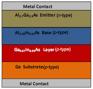
Abstract: In this paper, efficiency variation with change in device parameters (layer thickness and doping concentration) has been investigated in an Al0.7Ga0.3As/Al0.48In0.52As heterojunction solar cell using Adept 1D simulation software. The device uses a n-type Al0.7Ga0.3As top layer (Emitter), a p-type Al0.48In0.52As middle layer (Base),and a p-type Ga0.67In0.33As bottom layer, which, under high doping, acts as a passivating (BSF) layer. Germanium (Ge) substrate (p-doped) is used for the structure. Variation in efficiency is plotted against a particular changing parameter, keeping every other parameter fixed at some default value. After analyzing the variation curves, two optimized designs have been proposed, which yield 19.57% and 20.56% efficiency, respectively.
Numerical analysis of ultra thin high efficiency Cd1-xZnxS/Cd1-xZnxTe solar cell[edit | edit source]
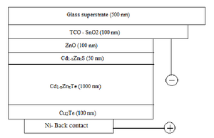
Authors: Mohammad Tanvirul Ferdaous, Md. Fokhrul Islam, K. A. S. M. Ehteshamul Haquev(Me), Nowshad Amin
Electrical and Electronic Engineering (Scientific and Academic Publishing) 2015, 5(1A): 14-18. DOI: 10.5923/c.eee.201501.03
Link: http://article.sapub.org/10.5923.c.eee.201501.03.html
Abstract: In this work, a new structure of CdS/CdTe based solar cell is proposed, where two of the fundamental drawbacks of traditional CdS/CdTe are addressed. The relatively low bandgap of CdS window layer, along with a significant lattice mismatch between CdS and CdTe lower the efficiency of conventional CdS/CdTe solar cell. This work proposes a novel structure where both window (CdS) and absorber (CdTe) layer are replaced by two II-VI ternary alloys, namely, Cd1-xZnxS and Cd1-xZnxTe respectively. These alloys give advantage of variable bandgap by varying Zn concentration in the alloys.A new structure of TCO/ZnO/Cd1-xZnxS/Cd1-xZnxTe/Cu2Te/Ni is proposed, which can easily be achieved by only changing S to Te during various fabrication processes. Numerical analysis was performed with AMPS 1D software and an efficiency of 24.643% was achieved through bandgap engineering, which is higher than the conventional CdS/CdTe solar cell. The solar cell was also found to be stable at higher temperature.
Conclusions[edit | edit source]
New materials and technologies are continuously investigated now for enhancing solar cell efficiency, and for reducing its cost. Solar cells have the potential for replacing the large-scale utilization of fossil fuels for electricity generation in today's world. However, the cost per unit (electricity) in case of solar cells is still higher than that of fossil fuels. This is actually keeping the solar cell research alive, and we can hope that we will breathe in a clean energy world someday.
References[edit | edit source]
Contact details[edit | edit source]
K A S M Ehteshamul Haque
showmo22@iut-dhaka.edu