J.M.Pearce (talk | contribs) m (→See also) |
|||
| (39 intermediate revisions by 4 users not shown) | |||
| Line 1: | Line 1: | ||
{{MOST}} | {{MOST}} | ||
[[category: MOST methods]] | [[category: MOST methods]] | ||
==Introduction== | ==Introduction== | ||
Photoluminescence{{w|Photoluminescence}} is the process where a substance absorbs photons and re-emits photons. The incident photons excite electrons from a lower energy level to a higher energy level. As the electrons relax from the higher energy level to the lower energy level a photon is released. For a [[semiconductor]], the electrons are excited from a set of energy levels called the [[valence band]] to a higher set of energy levels called the [[conduction band]]. The energy area between the valence band and the conduction band is called the [[band gap]], and no electrons can be energetically found here. | |||
'''Photoluminescence (PL) Spectroscopy''' is a type of contactless and nondestructive probing method for determining the electronic structure of a sample. In PL Spectroscopy, a [[laser]] is fired at a sample and the resulting fluorescence is measured by a [[spectrometer]]. The measured fluorescence can be used to determine the band gap of a semiconductor sample, impurity levels and possible defects in the sample, and the recombination mechanisms within the sample [http://www.nrel.gov/pv/measurements/photoluminescence_spectroscopy.html]. The determination of the electronic band gap for a semiconductor is the primary focus of this work. | |||
As previously stated, in a semiconductor the electrons are excited from the valence to the conduction band. When electrons relax from the conduction band back down to the valence band, photons will be released. '''These photons will have energy that matches the transition from the conduction band to the valence band. Measuring the emitted photons’ wavelength with a spectrometer will reveal the energy of the photon and therefore the size of the bandgap.''' | |||
== Design == | == Design == | ||
* | === Equipment List === | ||
*Design | *Pavilion Integration Corp W445-40FS 445 nm laser - 500mW | ||
[[image:ZIC 002.jpg|thumb|Laser linear response]] | |||
*Thor Labs LB1761-A N-BK7 Bi-Convex Lens, Ø1", f = 25.4 mm, Anit-Reflective Coating: 350-700nm | |||
*Thor Labs KM100-E02 Kinematic Mount for Ø1" Optics with Visible Laser Quality Mirror | |||
*Ocean Optics USB2000+VIS-NIR spectrometer, NIRQuest 512-2.5 | |||
*Ocean Optics 600 micron VIS NIR fiber optics cable part # QP600-2-VIS-NIR | |||
*[[open-source_optics_base|Open-Source Optics Base]] | |||
*[[open-source_simple_semiconductor_sample_holder|Open-Source Simple Semiconductor Sample]] | |||
*[[open-source_lens_holder|Open-Source Lens Holder]] | |||
*[[open-source_mirror_mount|Open-Source Mirror Mount]] | |||
*[[open-source_fiber_optic_cable_holder|Open-Source Fiber Optic Cable]] | |||
===Design Schematic=== | |||
[[Image:Open-source-PL_setup.png]] | |||
[[Image:PL-test-bench.jpg|thumb|left|Fig 1. The PL Test Bench]] | |||
[[Image:PL-setup.jpg|thumb|left|Fig 2. The PL Setup]] | |||
===Design Considerations and Explanations=== | |||
The first step to using of PL spectroscopy is to have a powerful enough laser to excite the electrons from the valence band to the conduction band for all the different samples you wish to examine. We used at 450 nm (2.755 eV) laser to test samples. This will only work for semiconductors with bandgaps smaller than 2.755eV. When choosing a laser, it is the wavelength that is important with intensity being a secondary concern since it is the wavelength that determines if the electrons jump the band gap. | |||
The setup of the PL system was designed from two separate works from the University of Colorado [http://www.physics.ohio-state.edu/~reu/99reu/final_reports/paper_hall.PDF] and from the University of Ohio [http://www.physics.ohio-state.edu/~reu/99reu/final_reports/paper_hall.PDF]. While researching the design of a PL system, it became obvious that researchers in general do not share their exact PL system design. Both of the works feature explicit diagrams of their photoluminescence spectroscopy setups. This open source PL spectroscopy setup is largely based on their previous work. | |||
Both of the setups from Colorado and OSU used a neutral density filter. We do not use one here because our laser has a variable intensity dial on it. The use of a mirror to bounce the laser onto the sample instead of direct illumination from the laser offers more flexibility. It is much easier to adjust the mirror than the laser. The laser is incident on the sample at a glancing angle so that specular reflection from the sample does not go near the fiber optic cable. This will reduce the laser signal read on the spectrometer and thus the noise. The spectrometer will still read some of the laser signal from diffuse reflection. The focusing lens is used to gather the fluorescence from the sample and focus it onto the fiber optic cable. Thus the fiber optic cable must be placed away from the lens at a distance equal to the focal length of the lens. The whole PL experiment is done within a dark box to limit the effect of outside light on the spectrometer. | |||
The mirror, sample, lens, and fiber optic cable are held in place with [[open source optics]] holders, which can be printed on an [[open source 3D printer]]. These open source optic holders allow us greater flexibility of placement than an optical bread board or lab bench would. However, it does lower the overall stability of the system, but such fined tuned stability is not needed for a simple PL system like this. | |||
== | ===Improvements=== | ||
There many improvements to this simple system that could be implemented. | |||
[[image:Sampleh3.jpg|thumb|left|Fig. 3. Open-source sample holder v3]] | |||
[[image:Switcher.jpg|thumb|right|Fig. 4. Open-source fiber switcher]] | |||
[[image:Rail.JPG|thumb|left|Fig. 5. Open-source rail]] | |||
* Shown on the left is an improved open-source sample holder for pieces of semiconductor wafers . Instead of the clamping a sample, it provides a 2mm lip that allows samples to fluently sink into the slot. The purpose of the design is to make sample switching faster and easier, and reduce abrasion caused by frequent sample switch. Also notice the hemisphere hole in the backside makes it easier for tweezers work. The design can be applied to variety of wafer-like material, we also use it as a mirror holder since it works fine with our appropediately sized mirror. | |||
* | * On the right is the improved fiber holder is a dual-channel fiber switcher, which attaches two fiber optic cable to a 8mm smooth rod and allow easy switching between cables for optical experiments. | ||
* In order to smoothly move each parts in our PL system, we've designed an optical rail that helps accurately align our system in a line and make lens focusing much easier. Installed with strong magnet the rail is clinging to the platform firmly. Now the system works in a fixed X-Y plane with measurable precision. | |||
==== Further improvement ==== | |||
* A component for a low temperature liquid to cool the sample during data taking. | |||
* The addition of a optical chopper and lock-in amplifier would improve signal to noise ratio | |||
* A monochromator would allow the system to focus on a small range of wavelengths at a time instead of looking a wide range of wavelengths. | |||
As part of the open source optics project we will be designing all of these components. | |||
== | == To operate == | ||
* [[Spectrometer and light source calibration: MOST]] | |||
[[category:open source optics]] | |||
== | == See also == | ||
* [[Photoluminescence protocol:QAS]] | |||
* [[PL data curve fitting:QAS]] | |||
* [[Photoluminescence literature review]] | |||
* Zhang C, Anzalone NC, Faria RP, Pearce JM (2013) [[Open-Source 3D-Printable Optics Equipment]]. ''PLoS ONE'' 8(3): e59840. doi:10.1371/journal.pone.0059840 [http://www.plosone.org/article/info%3Adoi%2F10.1371%2Fjournal.pone.0059840 open access] | |||
Revision as of 01:10, 28 March 2013
Introduction
PhotoluminescenceW is the process where a substance absorbs photons and re-emits photons. The incident photons excite electrons from a lower energy level to a higher energy level. As the electrons relax from the higher energy level to the lower energy level a photon is released. For a semiconductor, the electrons are excited from a set of energy levels called the valence band to a higher set of energy levels called the conduction band. The energy area between the valence band and the conduction band is called the band gap, and no electrons can be energetically found here.
Photoluminescence (PL) Spectroscopy is a type of contactless and nondestructive probing method for determining the electronic structure of a sample. In PL Spectroscopy, a laser is fired at a sample and the resulting fluorescence is measured by a spectrometer. The measured fluorescence can be used to determine the band gap of a semiconductor sample, impurity levels and possible defects in the sample, and the recombination mechanisms within the sample [1]. The determination of the electronic band gap for a semiconductor is the primary focus of this work.
As previously stated, in a semiconductor the electrons are excited from the valence to the conduction band. When electrons relax from the conduction band back down to the valence band, photons will be released. These photons will have energy that matches the transition from the conduction band to the valence band. Measuring the emitted photons’ wavelength with a spectrometer will reveal the energy of the photon and therefore the size of the bandgap.
Design
Equipment List
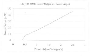
- Pavilion Integration Corp W445-40FS 445 nm laser - 500mW
- Thor Labs LB1761-A N-BK7 Bi-Convex Lens, Ø1", f = 25.4 mm, Anit-Reflective Coating: 350-700nm
- Thor Labs KM100-E02 Kinematic Mount for Ø1" Optics with Visible Laser Quality Mirror
- Ocean Optics USB2000+VIS-NIR spectrometer, NIRQuest 512-2.5
- Ocean Optics 600 micron VIS NIR fiber optics cable part # QP600-2-VIS-NIR
- Open-Source Optics Base
- Open-Source Simple Semiconductor Sample
- Open-Source Lens Holder
- Open-Source Mirror Mount
- Open-Source Fiber Optic Cable
Design Schematic

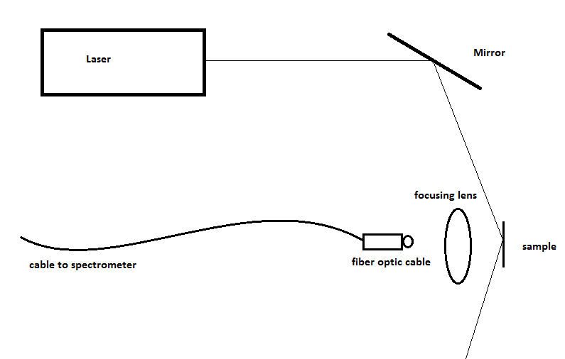
Design Considerations and Explanations
The first step to using of PL spectroscopy is to have a powerful enough laser to excite the electrons from the valence band to the conduction band for all the different samples you wish to examine. We used at 450 nm (2.755 eV) laser to test samples. This will only work for semiconductors with bandgaps smaller than 2.755eV. When choosing a laser, it is the wavelength that is important with intensity being a secondary concern since it is the wavelength that determines if the electrons jump the band gap.
The setup of the PL system was designed from two separate works from the University of Colorado [2] and from the University of Ohio [3]. While researching the design of a PL system, it became obvious that researchers in general do not share their exact PL system design. Both of the works feature explicit diagrams of their photoluminescence spectroscopy setups. This open source PL spectroscopy setup is largely based on their previous work.
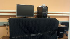
Both of the setups from Colorado and OSU used a neutral density filter. We do not use one here because our laser has a variable intensity dial on it. The use of a mirror to bounce the laser onto the sample instead of direct illumination from the laser offers more flexibility. It is much easier to adjust the mirror than the laser. The laser is incident on the sample at a glancing angle so that specular reflection from the sample does not go near the fiber optic cable. This will reduce the laser signal read on the spectrometer and thus the noise. The spectrometer will still read some of the laser signal from diffuse reflection. The focusing lens is used to gather the fluorescence from the sample and focus it onto the fiber optic cable. Thus the fiber optic cable must be placed away from the lens at a distance equal to the focal length of the lens. The whole PL experiment is done within a dark box to limit the effect of outside light on the spectrometer.
The mirror, sample, lens, and fiber optic cable are held in place with open source optics holders, which can be printed on an open source 3D printer. These open source optic holders allow us greater flexibility of placement than an optical bread board or lab bench would. However, it does lower the overall stability of the system, but such fined tuned stability is not needed for a simple PL system like this.
Improvements
There many improvements to this simple system that could be implemented.
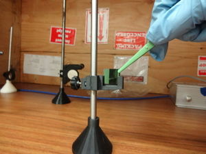
- Shown on the left is an improved open-source sample holder for pieces of semiconductor wafers . Instead of the clamping a sample, it provides a 2mm lip that allows samples to fluently sink into the slot. The purpose of the design is to make sample switching faster and easier, and reduce abrasion caused by frequent sample switch. Also notice the hemisphere hole in the backside makes it easier for tweezers work. The design can be applied to variety of wafer-like material, we also use it as a mirror holder since it works fine with our appropediately sized mirror.
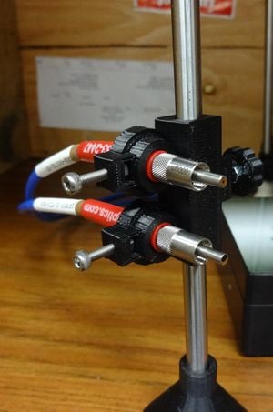
- On the right is the improved fiber holder is a dual-channel fiber switcher, which attaches two fiber optic cable to a 8mm smooth rod and allow easy switching between cables for optical experiments.
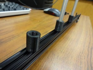
- In order to smoothly move each parts in our PL system, we've designed an optical rail that helps accurately align our system in a line and make lens focusing much easier. Installed with strong magnet the rail is clinging to the platform firmly. Now the system works in a fixed X-Y plane with measurable precision.
Further improvement
- A component for a low temperature liquid to cool the sample during data taking.
- The addition of a optical chopper and lock-in amplifier would improve signal to noise ratio
- A monochromator would allow the system to focus on a small range of wavelengths at a time instead of looking a wide range of wavelengths.
As part of the open source optics project we will be designing all of these components.
To operate
See also
- Photoluminescence protocol:QAS
- PL data curve fitting:QAS
- Photoluminescence literature review
- Zhang C, Anzalone NC, Faria RP, Pearce JM (2013) Open-Source 3D-Printable Optics Equipment. PLoS ONE 8(3): e59840. doi:10.1371/journal.pone.0059840 open access


