As we all know that the photovoltaic industry is growing at an astonishing speed and by the end of 2012, 100 GW was already installed worldwide [1]. It has now been confirmed that solar photovoltaics is the third most important renewable energy source after hydro and wind power. With that being said there is a emerging necessity for us to analyse the solar cell materials that have been commercialized. This analysis could give us an estimated idea of the best material available in terms of availability, cost, material thickness, environmental hazards, cost for recycling and many mare. With this idea in mind, I worked on it, with the available literature. The consolidated data can be found here: Literature Review on Photovoltaic Materials
On the basis of the literature review, I had to compare all the commercialized solar cells ie c-Si, a-Si, Cadmium Telluride and CIGS. I had to find out the materials used in the cell for a particular design and in what quantities it was used. Knowing the materials used in the cells, it is very important to know the reserves available to us in the lithosphere of a particular material. For example crystalline silicon is used in monocrystalline and multicrystalline solar cells and it is well established that it is the second most abundantly available material in earth's crust.Abundance of materials[1] Also in these designs, a critical factor is the thickness of the materials used i.e the more thicker the layer the more material is required. For this analysis, the cell design was considered by me in each of the above technologies. My effort here was to find out the designs which were most recent with the highest conversion efficiency available in each of the technologies so as to know the current state of the art in photovoltaic industry.
Crystalline silicon solar cell
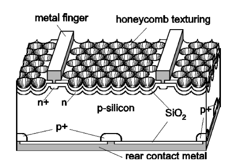
19.8% efficient ‘‘honeycomb’’ textured multicrystalline and 24.4% monocrystalline silicon solar cells[2]
Zhao et al showed in this paper that "honeycomb" texturing help in increasing the efficiency. Especially the previous monocrystalline device which had the efficiency of 24% made use of "inverted pyramid" which are formed due to anisotropic etching to expost intersecting {111} crystal plane. There is also a very thin layer of SiO2 used so as to keep the recombination losses in oxide covered area to be low. Very narrow slots of the order of few microns are opens to make contacts of the finger contacts with the highly doped n type region while small opening are made for the back contact with the p type material. The reason for these narrow openings are to reduce contact resistance and recombination by suppressing minority carrier concentration near the contact. With the novel honeycomb texturing cascaded with the inverted pyradmids a cell efficiency of 24.4% was achieved successfully. With the cell design used the thickness of crystalline material used is 260 microns.
For this cell the total area device parameters are as follows under AM1.5 test conditions:
- open-circuit voltage (Voc)=643mV
- short circuit current density (Jsc)=42 mA/cm2
- fill factor (FF)=83.6%
- efficiency=24.4%
- device area=4 cm2.
The below figure shows the c-Si solar cell.

Amorphous silicon solar cell
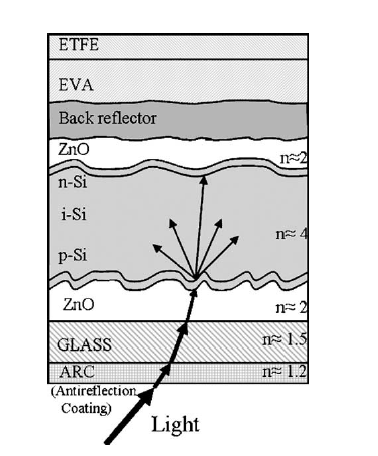
Towards very low-cost mass production of thin-film silicon photovoltaic (PV) solar modules on glass[3]
HIGH-EFFICIENCY AMORPHOUS SILICON DEVICES ON LPCVD-ZNO TCO PREPARED IN INDUSTRIAL KAITM-M R&D REACTOR[4]
The above two literature references from which the model used in A. Shah et al [3] has been taken as the reference solar cell for a-Si technology. Also a study done by S. Benagli et al [4] presented results on optimal i-layer thickness for amorphous silicon solar cell using p-i-n type deposited on doped LPCVD-ZnO. The i-layer thickness is kept very low of the order from 150 to 300nm, because of the light induced degradation effect, that reduces collection length by adversely affecting the mobility x lifetime product and the internal electric field witin the photoactive i layer [3]. A common feature to all thin film solar cell is that Transparent Conductive Oxide (TCO) is used as a transparent electrode on the side where the light enters the solar cell. The TCO is generally deposited over glass substrate. Surface texturing help the TCO layer to achieve additional scattering of incoming light. The backreflector (typically Al or Ag) ensure light trapping within the solar cell. The i-layer thickness of the cell used was 250nm with ZnO type B which gave a recored efficiency of 10.09% confirmed by NREL.
For this cell the total area device parameters are as follows under AM1.5 test conditions:
- open-circuit voltage (Voc)=0.8767V
- short circuit current density (Jsc)=17.284 mA/cm2
- fill factor (FF)=66.58%
- efficiency=10.09%
- device area=1.047 cm2.
Cadmium telluride solar cell
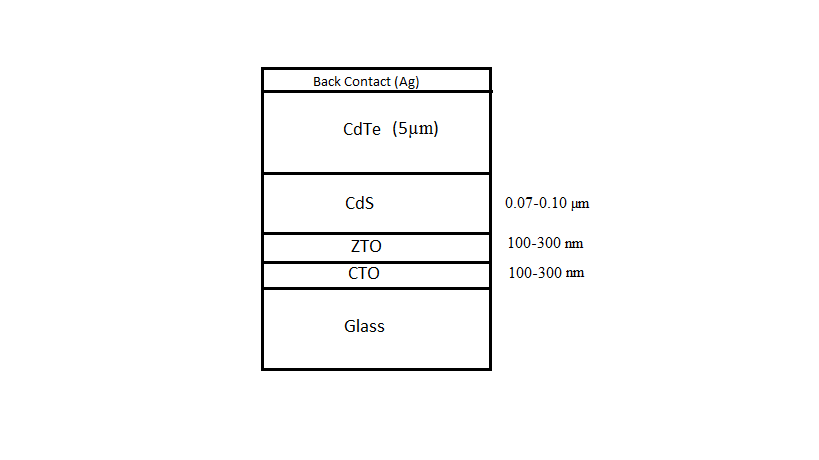
High-Efficiency CTO/ZTO/CdS/CdTe Polycrystalline Thin-Film Solar Cells[5]
Thin‐film CdS/CdTe solar cell with 15.8% efficiency[6]
For the Cadmium Telluride solar cells, the structure formed by X. Wu et al [5] gave an efficiency of 16.5% and a Fill Factor (FF) of 75.51%. In this structure different kind of TCO's are developed which are Cadmium stannate (Cd2SnO4) or CTO and Zinc stannate (Zn2SnO4) or ZTO. The advantages of CTO over conventional SnO2 Tco films are its lower resistivity, higher transmittance and smoother surfaces. It has been shown that when CTO is introduced in the CdTe solar cells, Jsc and FF both can be improved. The purpose of integrating high resistivity ZTO layer was to improve device performance and reproduceability. The thickness of these 2 layers varies between 100 to 300 nm. To improve the blue quantum efficiency and Jsc further, they developed and integrated modified CdS film with higher bandgap into the device which facilitated high efficiency CdS/CdTe polycrystalline thin film solar cells. The thickness of material was described in J Britt and C Ferekides with CdS layer thickness of 0.07µm to 0.10µm and CdTe layer thickness was defined to be 5 µm [6].
For this cell the total area device parameters are as follows under AM1.5 test conditions:
- open-circuit voltage (Voc)=845mV
- short circuit current density (Jsc)=25.88 mA/cm2
- fill factor (FF)=75.51%
- efficiency=16.5%
- device area=1.032 cm2.
CIGS solar cell
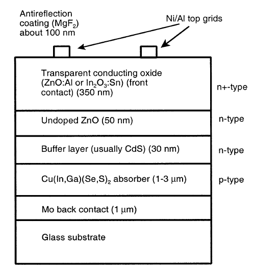
19·9%-efficient ZnO/CdS/CuInGaSe2 solar cell with 81·2% fill factor[7]
In the CIGS device, the research work done my I. Repins et al [7] in developing the model with CIGS thickness of 2.2 µm having a world record efficiency of 19.9% and the highest FF of 81.2% was achieved. The previous record was of 19.5% in which the CIGS layer thickness was 2.7 µm. However the researchers confirmed that the improved performance was due to decreased recombination and not due to the reduced thickness. 3 steps were varied than the previous device which are described as follows:
- During the deposition process, Ga and In were delivered in the typical Ga/(In+Ga)~ 0.3 ratio. However In thickness of about 25 angstroms was deposited in the absence of Ga in the last 10 seconds.
- After the deposition process, the model was annealed with Se at 600˚C for 2.5 mins.
- A 2-min, 200˚C air anneal was performed after the CdS deposition. It is to be noted that from the previous device, this step was completely eliminated of Ga.
With these 3 process flow change step than the previous device, the recombination rate was reduced at the surface of CIGS cell.
For this cell the total area device parameters are as follows under AM1.5 test conditions:
- open-circuit voltage (Voc)=0.690V
- short circuit current density (Jsc)=35.5 mA/cm2
- fill factor (FF)=81.2%
- efficiency=19.9%
- device area=0.419 cm2.
Equations used for mathematical analysis
- The mass (m) in g is given by:
m = A x tc x d
where A is the area in m2, tc is the cell thickness in m, and d is the density in g/cm3.
- The efficiency (ƞ) in %is given by:
ƞglobal = [iph x Voc x FF]/Is
where iph is photocurrent density in mA/cm2, Voc is open-circuit voltage in V, FF is fill factor in % and Is is the intensity of incident light in W/m2
- Th maximum power (Pmax) in W is given by:
(Pmax) = ƞglobal x Is x A
where ƞglobal is the efficiency in %, Is is the intensity of incident light in W/m2 and where A is the area in m2.
References
- ↑ http://www.webelements.com/silicon/geology.html
- ↑ Zhao, Jianhua, Aihua Wang, Martin A. Green, and Francesca Ferrazza. “19.8% Efficient ‘honeycomb’ Textured Multicrystalline and 24.4% Monocrystalline Silicon Solar Cells.” Applied Physics Letters 73, no. 14 (October 5, 1998): 1991–1993. doi:10.1063/1.122345.
- ↑ Shah, A., J. Meier, A. Buechel, U. Kroll, J. Steinhauser, F. Meillaud, H. Schade, and D. Dominé. “Towards Very Low-Cost Mass Production of Thin-Film Silicon Photovoltaic (PV) Solar Modules on Glass.” Thin Solid Films 502, no. 1–2 (April 28, 2006): 292–299. doi:10.1016/j.tsf.2005.07.299.
- ↑ S Benagli, D. Borrello. “High-Efficiency Amorphous Silicon Devices on LPCVD-ZnO TCO Prepared in Industrial KAI-M R&D Reactor.” 24th European Photovoltaic Solar Energy Conference, Hamburg (2009): 344–349.
- ↑ X. Wu, R.G. Dhere. "High-Efficiency CTO/ZTO/CdS/CdTe Polycrystalline Thin-Film Solar Cells", National Renewable Energy Laboratory (NREL), NCPV Program Review Meeting Lakewood, Colorado.
- ↑ Britt, J., and C. Ferekides. “Thin‐film CdS/CdTe Solar Cell with 15.8% Efficiency.” Applied Physics Letters 62, no. 22 (May 31, 1993): 2851–2852. doi:10.1063/1.109629.
- ↑ Repins, Ingrid, Brian Egaas, Clay DeHart, John Scharf, Craig L. Perkins, Bobby To, and Rommel Noufi. “19·9%-Efficient ZnO/CdS/CuInGaSe2 Solar Cell with 81·2% Fill Factor.” Progress in Photovoltaics: Research and Applications 16, no. 3 (2008): 235–239. doi:10.1002/pip.822.
See also
Interwiki links
- Wikipedia:
- []
External links
- []
[[Category:]] [[Category:]]


