J.M.Pearce (talk | contribs) m (→See Also) |
J.M.Pearce (talk | contribs) m (→See Also) |
||
| Line 24: | Line 24: | ||
* [[Enhancement of hydrogenated amorphous silicon solar cells with front-surface hexagonal plasmonic arrays from nanoscale lithography]] | * [[Enhancement of hydrogenated amorphous silicon solar cells with front-surface hexagonal plasmonic arrays from nanoscale lithography]] | ||
* [[Fabricating Ordered 2-D Nano-Structured Arrays Using Nanosphere Lithography]] | * [[Fabricating Ordered 2-D Nano-Structured Arrays Using Nanosphere Lithography]] | ||
* [[Scalable honeycomb top contact to increase the light absorption and reduce the series resistance of thin film solar cells]] | |||
{{Solar navbox}} | {{Solar navbox}} | ||
Revision as of 00:56, 20 December 2018

Source
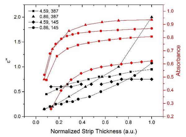
- Wyatt Adams, Ankit Vora, Jephias Gwamuri, Joshua M. Pearce, Durdu Ö. Guney. Controlling optical absorption in metamaterial absorbers for plasmonic solar cells. Proc. SPIE 9546, Active Photonic Materials VII, 95461M (August 31, 2015); doi:10.1117/12.2190396. open access
Abstract
Metals in the plasmonic metamaterial absorbers for photovoltaics constitute undesired resistive heating. However, tailoring the geometric skin depth of metals can minimize resistive losses while maximizing the optical absorbance in the active semiconductors of the photovoltaic device. Considering experimental permittivity data for InxGa1-xN, absorbance in the semiconductor layers of the photovoltaic device can reach above 90%. The results here also provides guidance to compare the performance of different semiconductor materials. This skin depth engineering approach can also be applied to other optoelectronic devices, where optimizing the device performance demands minimizing resistive losses and power consumption, such as photodetectors, laser diodes, and light emitting diodes.
Keywords
Absorption ; Metamaterials ; Solar cells ; Semiconductors ; Skin ; Absorbance ; Metals ; Engineering ; Light emitting diodes ; Optoelectronic devices
See Also
- Advances in plasmonic light trapping in thin-film solar photovoltaic devices
- Plasmonic Perfect Meta-Absobers for a-Si PV Devices
- Limitations of ultra-thin transparent conducting oxides for integration into plasmonic-enhanced thin-film solar photovoltaic devices
- Optical modelling of thin film microstructures literature review
- Multi-resonant silver nano-disk patterned thin film hydrogenated amorphous silicon solar cells for Staebler-Wronski effect compensation
- Influence of Oxygen Concentration on the Performance of Ultra-Thin RF Magnetron Sputter Deposited Indium Tin Oxide Films as a Top Electrode for Photovoltaic Devices
- A new method of preparing highly conductive ultra-thin indium tin oxide for plasmonic-enhanced thin film solar photovoltaic devices
- Plasmonic enhancement of amorphous silicon solar photovoltaic cells with hexagonal silver arrays made with nanosphere lithography
- Enhancement of hydrogenated amorphous silicon solar cells with front-surface hexagonal plasmonic arrays from nanoscale lithography
- Fabricating Ordered 2-D Nano-Structured Arrays Using Nanosphere Lithography
- Scalable honeycomb top contact to increase the light absorption and reduce the series resistance of thin film solar cells


