J.M.Pearce (talk | contribs) (Created page with "{{MOST}} {{Pearce-pubs}} right|400px ==Source== Marikkannan, M. and Vishnukanthan, V. and Vijayshankar, A. and Mayandi, J. and Pearce, J. M., A novel synthe...") |
J.M.Pearce (talk | contribs) m (→See Also) |
||
| (6 intermediate revisions by the same user not shown) | |||
| Line 4: | Line 4: | ||
[[image:Ito.gif|right|400px]] | [[image:Ito.gif|right|400px]] | ||
==Source== | ==Source== | ||
Marikkannan, M. | * Marikkannan, M., Vishnukanthan, V., Vijayshankar, A., Mayandi, J. and Pearce, J. M., A novel synthesis of tin oxide thin films by the sol-gel process for optoelectronic applications.''AIP Advances'', '''5''', 027122 (2015), DOI:http://dx.doi.org/10.1063/1.4909542 [https://www.academia.edu/10848713/A_novel_synthesis_of_tin_oxide_thin_films_by_the_sol-gel_process_for_optoelectronic_applications open access] | ||
==Abstract== | ==Abstract== | ||
| Line 11: | Line 11: | ||
==See Also== | ==See Also== | ||
*[[Effect of ambient combinations of argon, oxygen, and hydrogen on the properties of DC magnetron sputtered indium tin oxide films]] | *[[Effect of ambient combinations of argon, oxygen, and hydrogen on the properties of DC magnetron sputtered indium tin oxide films]] | ||
*[[A new method of preparing highly conductive ultra-thin indium tin oxide for plasmonic-enhanced thin film solar photovoltaic devices]] | |||
*[[Advances in plasmonic light trapping in thin-film solar photovoltaic devices]] | *[[Advances in plasmonic light trapping in thin-film solar photovoltaic devices]] | ||
*[[Limitations of ultra-thin transparent conducting oxides for integration into plasmonic-enhanced thin-film solar photovoltaic devices]] | |||
*[[Plasmonic Perfect Meta-Absobers for a-Si PV Devices]] | *[[Plasmonic Perfect Meta-Absobers for a-Si PV Devices]] | ||
*[[Optical modelling of thin film microstructures literature review]] | *[[Optical modelling of thin film microstructures literature review]] | ||
*[[Multi-resonant silver nano-disk patterned thin film hydrogenated amorphous silicon solar cells for Staebler-Wronski effect compensation]] | *[[Multi-resonant silver nano-disk patterned thin film hydrogenated amorphous silicon solar cells for Staebler-Wronski effect compensation]] | ||
*[[Influence of Oxygen Concentration on the Performance of Ultra-Thin RF Magnetron Sputter Deposited Indium Tin Oxide Films as a Top Electrode for Photovoltaic Devices]] | |||
* [[Ambiance-dependent Agglomeration and Surface-enhanced Raman Spectroscopy Response of Self-assembled Silver Nano-particles for Plasmonic Photovoltaic Devices]] | |||
* [[Scalable honeycomb top contact to increase the light absorption and reduce the series resistance of thin film solar cells]] | |||
{{Solar navbox}} | |||
[[Category:MOST completed projects and publications]] | [[Category:MOST completed projects and publications]] | ||
Revision as of 00:58, 20 December 2018

Source
- Marikkannan, M., Vishnukanthan, V., Vijayshankar, A., Mayandi, J. and Pearce, J. M., A novel synthesis of tin oxide thin films by the sol-gel process for optoelectronic applications.AIP Advances, 5, 027122 (2015), DOI:http://dx.doi.org/10.1063/1.4909542 open access
Abstract
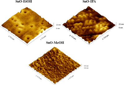
A novel and simple chemical method based on sol-gel processing was proposed to deposit metastable orthorhombic tin oxide (SnOx) thin films on glass substrates at room temperature. The resultant samples are labeled according to the solvents used: ethanol (SnO-EtOH), isopropanol (SnO-IPA) and methanol (SnO-MeOH). The variations in the structural, morphological and optical properties of the thin films deposited using different solvents were characterized by X-ray diffraction, atomic force microscopy, Raman spectroscopy, Fourier transform infrared (FTIR) spectroscopy, UV-vis spectroscopy and photoluminescence (PL) analysis. The XRD patterns confirm that all the films, irrespective of the solvents used for preparation, were polycrystalline in nature and contained a mixed phases of tin (II) oxide and tin (IV) oxide in a metastable orthorhombic crystal structure. FTIR spectra confirmed the presence of Sn=O and Sn-O in all of the samples. PL spectra showed a violet emission band centered at 380 nm (3.25 eV) for all of the solvents. The UV-vis spectra indicated a maximum absorption band shown at 332 nm and the highest average transmittance around 97% was observed for the SnO-IPA and SnO-MeOH thin film samples. The AFM results show variations in the grain size with solvent. The structural and optical properties of the SnO thin films indicate that this method of fabricating tin oxide is promising and that future work is warranted to analyze the electrical properties of the films in order to determine the viability of these films for various transparent conducting oxide applications.
See Also
- Effect of ambient combinations of argon, oxygen, and hydrogen on the properties of DC magnetron sputtered indium tin oxide films
- A new method of preparing highly conductive ultra-thin indium tin oxide for plasmonic-enhanced thin film solar photovoltaic devices
- Advances in plasmonic light trapping in thin-film solar photovoltaic devices
- Limitations of ultra-thin transparent conducting oxides for integration into plasmonic-enhanced thin-film solar photovoltaic devices
- Plasmonic Perfect Meta-Absobers for a-Si PV Devices
- Optical modelling of thin film microstructures literature review
- Multi-resonant silver nano-disk patterned thin film hydrogenated amorphous silicon solar cells for Staebler-Wronski effect compensation
- Influence of Oxygen Concentration on the Performance of Ultra-Thin RF Magnetron Sputter Deposited Indium Tin Oxide Films as a Top Electrode for Photovoltaic Devices
- Ambiance-dependent Agglomeration and Surface-enhanced Raman Spectroscopy Response of Self-assembled Silver Nano-particles for Plasmonic Photovoltaic Devices
- Scalable honeycomb top contact to increase the light absorption and reduce the series resistance of thin film solar cells


