Faiza Anjum (talk | contribs) (Deposition of Indium and Gallium based Nitrides thin films using plasma research) |
Faiza Anjum (talk | contribs) No edit summary |
||
| (One intermediate revision by the same user not shown) | |||
| Line 1: | Line 1: | ||
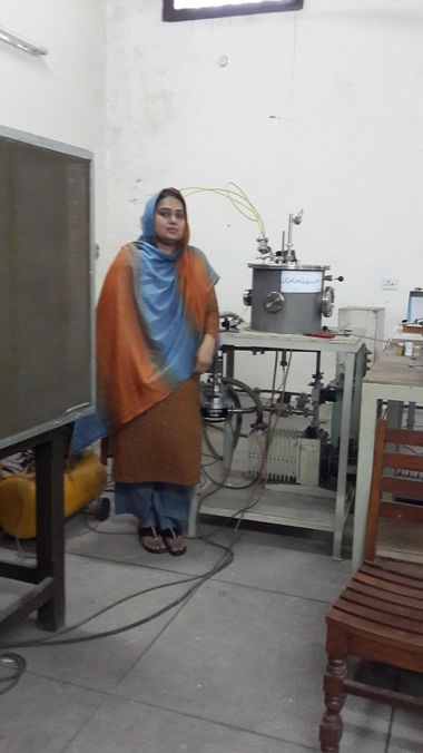
[[Image:Pic faiza.jpg|thumb|center|upright=1.25|Faiza Anjum is a PhD student at Department of Physics GC Univerisity Lahore Pakistan]] | |||
'' 'Bibliography'' | '' 'Bibliography'' | ||
Revision as of 12:34, 28 June 2016

'Bibliography
I am a PhD scholar at Department of Physics, GC University,Lahore-54000 Pakistan. The title of my PhD research work is " Thin film of indium nitride and gallium nitride using plasma. I have got a degree of Bachelor and Master of Science in 2002 and 2005 respectively from the Faculty of sciences at the Islamia University of Bahawalpur in Pakistan. I was awarded with 4th position in MSc from this University. I have got a degree of MPhil physics (18 year education) in 2008.In addition to my academic activities, I have also experienced a task of a teacher at university and college level. It helped me to develop a strong analytical mind and interpersonal skills. Moreover, I learned the value of teamwork and became more solution-oriented, adapting to a constantly changing work environment and maintaining good working relationships with individuals of different cultural backgrounds. currently I am the visiting factuality member of GC university Lahore Pakistan.
Research Interests
my research is about Deposition of Indium and Gallium based Nitrides thin films using plasma.In this research project, Indium and Gallium based Nitrides thin films would be deposited using different plasma sputtering techniques. The phase analysis and surface morphology will be investigated using XRD, SEM and AFM,. Mechanical properties will be examined using nano and microhardness indentation techniques. The thickness of the films will be studied by cross-sectional SEM analysis and elipsometry. The electrical properties will be studied by Hall Effect and using four-probe technique. The electrical characteristics of all samples will be conducted using Keithley's I–V measurement system. The optical properties will be studied by using elipsometer, UV VIS meter, Raman and Fourier FTIR spectroscopy.
Nitride semiconductors are viewed as highly promising material system for electronic and optoelectronic application. The group III nitrides (AlN, GaN and InN) represent an important trio of semiconductors because of their direct band gaps which span the range 1.95-6.2 eV, including the whole of the visible region and extending well out into the ultraviolet (UV) range. High brightness visible light-emitting diodes (LEDs),photodetectrors, photoconductors, charge-coupled devices, and photomultiplier tubes continuously operating UV laser diodes are now commercially available and of tremendous interest for high-density optical application.
As a member of III-nitrides family indium nitride has a remarkably narrow band gap, only 0.7 electron volts, which correspond to the near-infrared region of the electromagnetic spectrum. The narrow band gap means that indium nitride could find applications in highly efficient light-emitting diodes, laser diodes, and high-frequency transistors. Even more promising, when alloyed with gallium nitride, another member of group III nitride holds out the possibility of making extraordinary photodiode used in solar cells. Gallium nitride has a band gap of 3.4 electron volts, matching the high energy of the near-ultraviolet region of the spectrum. Thin film of indium, gallium and nitrogen alloyed in different proportions could be stacked in a solar cell that would span virtually the entire spectrum of sunlight, yielding a solar cell far more efficient than any yet made. Furthermore, recently several teams around the world deposited InN using Molecular Beam Epitaxy (MBE) and obtained infrared photoluminescence, photoreflectance and transmittance data that seems to indicate that the InN bandgap should lie in the 0.6 – 0.8 eV range, making InN a very interesting material for telecommunication applications.