J.M.Pearce (talk | contribs) m (→Source) |
(Set shorter title-tag for SEO purposes) |
||
| (29 intermediate revisions by 9 users not shown) | |||
| Line 1: | Line 1: | ||
{{ | {{Solar menu}} | ||
{{Pearce- | |||
[[File:Nanolith.jpg|thumb]] | |||
{{Source data | |||
| type = Paper | |||
| cite-as = Chenlong Zhang, Sandra Cvetanovic, Joshua M. Pearce. [https://doi.org/10.1016/j.mex.2017.07.001 Fabricating Ordered 2-D Nano-Structured Arrays Using Nanosphere Lithography]. ''MethodsX'' 4, 2017, pp. 229-242. DOI:10.1016/j.mex. [https://www.academia.edu/34554395/Fabricating_ordered_2-D_nano-structured_arrays_using_nanosphere_lithography open access] | |||
}} | |||
{{Project data | |||
| authors = Chenlong Zhang, Sandra Cvetanovic, J.M.Pearce | |||
| status = Designed, Modelled, Prototyped, Verified | |||
| verified-by = MOST | |||
| links = https://www.academia.edu/34554395/Fabricating_ordered_2_D_nano_structured_arrays_using_nanosphere_lithography|, https://www.sciencedirect.com/science/article/pii/S2215016117300213?via%3Dihub| | |||
| location = Michigan, USA | |||
}} | |||
{{Device data | |||
= | | design-files = https://www.youmagine.com/designs/dip-holder-for-nanosphere-lithography YouMagine.com | ||
}} | |||
{{MOST}} | |||
{{ | |||
Recent advances in the use of plasmonic metamaterials to improve absorption of light in thin-film solar photovoltaic devices has created a demand for a scalable method of patterning large areas with metal nanostructures deposited in an ordered array. This article describes two methods of fabricating ordered 2D nanosphere colloidal films: spin coating and interface coating. The two methods are compared and parameter optimization discussed. The study reveals that: | Recent advances in the use of plasmonic metamaterials to improve absorption of light in thin-film solar photovoltaic devices has created a demand for a scalable method of patterning large areas with metal nanostructures deposited in an ordered array. This article describes two methods of fabricating ordered 2D nanosphere colloidal films: spin coating and interface coating. The two methods are compared and parameter optimization discussed. The study reveals that: | ||
* For smaller nanosphere sizes, spin coating is more favorable, while for larger nanospheres, the angled interface coating provides more coverage and uniformity. | * For smaller nanosphere sizes, spin coating is more favorable, while for larger nanospheres, the angled interface coating provides more coverage and uniformity. | ||
* A surfactant-free approach for interface coating is developed to fabricate zero-contamination colloidal films. | * A surfactant-free approach for interface coating is developed to fabricate zero-contamination colloidal films. | ||
* Each of the methods reaches an overall coverage of more than 90% and can be used for nanosphere lithography to form plasmonic metamaterials. | * Each of the methods reaches an overall coverage of more than 90% and can be used for nanosphere lithography to form plasmonic metamaterials. | ||
* 3D printed parametric dipper https://www.youmagine.com/designs/dip-holder-for-nanosphere-lithography | |||
{{Pearce publications notice}} | |||
== | == Methods == | ||
Detailed methods in the paper - also supported by: | |||
* [[Perkin-Elmer RF Sputtering System-6 Inch protocol: MOST]] | * [[Perkin-Elmer RF Sputtering System-6 Inch protocol: MOST]] | ||
* [[Chenlong Nanobeads Project]] | * [[Chenlong Nanobeads Project]] | ||
==See | == See also == | ||
* [[Plasmonic enhancement of amorphous silicon solar photovoltaic cells with hexagonal silver arrays made with nanosphere lithography]] | * [[Plasmonic enhancement of amorphous silicon solar photovoltaic cells with hexagonal silver arrays made with nanosphere lithography]] | ||
*[[A new method of preparing highly conductive ultra-thin indium tin oxide for plasmonic-enhanced thin film solar photovoltaic devices]] | * [[A new method of preparing highly conductive ultra-thin indium tin oxide for plasmonic-enhanced thin film solar photovoltaic devices]] | ||
*[[Limitations of ultra-thin transparent conducting oxides for integration into plasmonic-enhanced thin-film solar photovoltaic devices]] | * [[Limitations of ultra-thin transparent conducting oxides for integration into plasmonic-enhanced thin-film solar photovoltaic devices]] | ||
*[[Influence of Oxygen Concentration on the Performance of Ultra-Thin RF Magnetron Sputter Deposited Indium Tin Oxide Films as a Top Electrode for Photovoltaic Devices]] | * [[Influence of Oxygen Concentration on the Performance of Ultra-Thin RF Magnetron Sputter Deposited Indium Tin Oxide Films as a Top Electrode for Photovoltaic Devices]] | ||
*[[Advances in plasmonic light trapping in thin-film solar photovoltaic devices]] | * [[Advances in plasmonic light trapping in thin-film solar photovoltaic devices]] | ||
*[[Controlling optical absorption in metamaterial absorbers for plasmonic solar cells]] | * [[Controlling optical absorption in metamaterial absorbers for plasmonic solar cells]] | ||
*[[Plasmonic Perfect Meta-Absobers for a-Si PV Devices]] | * [[Plasmonic Perfect Meta-Absobers for a-Si PV Devices]] | ||
*[[Multi-resonant silver nano-disk patterned thin film hydrogenated amorphous silicon solar cells for Staebler-Wronski effect compensation]] | * [[Multi-resonant silver nano-disk patterned thin film hydrogenated amorphous silicon solar cells for Staebler-Wronski effect compensation]] | ||
* [[Enhancement of hydrogenated amorphous silicon solar cells with front-surface hexagonal plasmonic arrays from nanoscale lithography]] | * [[Enhancement of hydrogenated amorphous silicon solar cells with front-surface hexagonal plasmonic arrays from nanoscale lithography]] | ||
* [[Optimal Design of Thin-film Plasmonic Solar Cells using Differential Evolution Optimization Algorithms]] | |||
* [[Scalable honeycomb top contact to increase the light absorption and reduce the series resistance of thin film solar cells]] | |||
{{Page data | |||
| title-tag = Fabricating Ordered 2-D Nano-Structured Arrays | |||
| keywords = microsphere lithography, nanosphere lithography, dip coating, spin coating, nanosphere, plasmonic, metamaterial, synthesis, Materials processing, Photovoltaics | |||
| sdg = SDG09 Industry innovation and infrastructure | |||
| organizations = MOST, MTU | |||
}} | |||
[[Category:MOST completed projects and publications]] | [[Category:MOST completed projects and publications]] | ||
[[Category:Materials]] | [[Category:Materials]] | ||
[[Category:Materials processing]] | [[Category:Materials processing]] | ||
[[Category:Photovoltaics]] | [[Category:Photovoltaics]] | ||
Latest revision as of 15:56, 23 February 2024

Recent advances in the use of plasmonic metamaterials to improve absorption of light in thin-film solar photovoltaic devices has created a demand for a scalable method of patterning large areas with metal nanostructures deposited in an ordered array. This article describes two methods of fabricating ordered 2D nanosphere colloidal films: spin coating and interface coating. The two methods are compared and parameter optimization discussed. The study reveals that:
- For smaller nanosphere sizes, spin coating is more favorable, while for larger nanospheres, the angled interface coating provides more coverage and uniformity.
- A surfactant-free approach for interface coating is developed to fabricate zero-contamination colloidal films.
- Each of the methods reaches an overall coverage of more than 90% and can be used for nanosphere lithography to form plasmonic metamaterials.
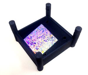
- 3D printed parametric dipper https://www.youmagine.com/designs/dip-holder-for-nanosphere-lithography
Methods[edit | edit source]
Detailed methods in the paper - also supported by:
See also[edit | edit source]
- Plasmonic enhancement of amorphous silicon solar photovoltaic cells with hexagonal silver arrays made with nanosphere lithography
- A new method of preparing highly conductive ultra-thin indium tin oxide for plasmonic-enhanced thin film solar photovoltaic devices
- Limitations of ultra-thin transparent conducting oxides for integration into plasmonic-enhanced thin-film solar photovoltaic devices
- Influence of Oxygen Concentration on the Performance of Ultra-Thin RF Magnetron Sputter Deposited Indium Tin Oxide Films as a Top Electrode for Photovoltaic Devices
- Advances in plasmonic light trapping in thin-film solar photovoltaic devices
- Controlling optical absorption in metamaterial absorbers for plasmonic solar cells
- Plasmonic Perfect Meta-Absobers for a-Si PV Devices
- Multi-resonant silver nano-disk patterned thin film hydrogenated amorphous silicon solar cells for Staebler-Wronski effect compensation
- Enhancement of hydrogenated amorphous silicon solar cells with front-surface hexagonal plasmonic arrays from nanoscale lithography
- Optimal Design of Thin-film Plasmonic Solar Cells using Differential Evolution Optimization Algorithms
- Scalable honeycomb top contact to increase the light absorption and reduce the series resistance of thin film solar cells


