Our team is investigating a way to print semiconductor transistors using 3D-printing technology. Specifically using Zinc Antimonide (ZnSb) as the semiconducting material for both the N-type and P-type semiconductor material for use in the transistor. The transistor itself is a small, relatively simple component used in modern electronic devices which can be built upon to create a wide variety of useful "smart" devices. Some possibilities include smart materials that can sense their environment, respond to signals the potential to provide processing capabilities, all within a package that could be readily generated in a home or hobby environment.
Background[edit | edit source]
Semiconductors are the backbone of modern electronic devices. There are numerous forms of semiconductors commonly found in everyday life such as computers, cell phones, calculators, LED light fixtures, automobiles and countless other applications. Semiconducting materials provide the means to create small, inexpensive, energy efficient devices that can perform a wide variety of functions. Consider the cell phone that shrank from a bulky bag phone of the 1980's to the flip phones of the 1990's to the multifunctional smart phones we use today. All of this is due to advances in the field of semiconductors.
With the rise in popularity of 3D printing, both from a commercial and hobby perspective, there is a great deal of interest in harnessing the inherent flexibility of 3D printing technology to not only generate complex shapes with additive manufacturing techniques, but to make those objects "smart". Many of these advancements are due to new and creative ways to fabricate transistors with smaller packages and greater reliability. Consider the possibility for components extruded from plastics or other materials with the ability to communicate with each other, provide conductive pathways for powering integrated components such as printed LED lights, displays and other functions.
Benefits of 3D Printing[edit | edit source]
The core benefit of using the 3D printing approach of electronic device creation is the flexibility of the process. Provided suitable materials and schematics are available it is possible to build any combination of devices. The transistor is a small but very potent part of this flexibility. Once a suitable transistor is designed, numerous electronic circuits of interest can then be fabricated such as logic gates, amplifying circuits and device control switches. Not only can these devices be created, they can be scaled to suit specific needs.
It would be possible then for a suitably equipped 3D printer to not only be able to print "smart" parts that could electronically interface with each other, but to also build control circuits used to run the printers. Some applications could include building control board for running newer versions of 3D printers that not only handle the operational control functions of running stepper motors and controlling current to the extrusion head, but also sensing capabilities that could be directly integrated into the components used to build the printers. integrating sensing circuits into printed components would allow for feedback signals that could permit higher quality parts to be printed with less waste due to part scrapping.
The Transistor[edit | edit source]
Transistors penetrate all levels of our society; they appear in our homes, our workplaces, our kitchens, our pockets. They have helped us go into space and into the depths of the ocean. They form the basis of any "smart" device. They are what make our electronic devices possible.
A transistor has three terminals: the base, the emitter, and the collector. Transistors control current flow; a small current flowing into the base controls a large current running through the collector and emitter.[1]
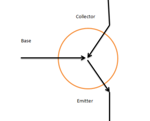
When the current flows into the base, as is shown in Figure 1, current will flow from the collector to the emitter, as is shown. The current is unable to flow the other direction. If the current flowing through the base is reversed, the large current will only be able to flow the other direction.
Method of Printing Transistors[edit | edit source]
The bulk of the 3D printed part can be constructed using traditional extrusion methods to build up the surfaces and component as desired. The printing of the transistor and associated trace leads would require the creation of a flat smooth surface. To achieve this desired surface after creating the plane where the transistor is to be located, several layers of polyurethane should be used to fill in small surface defects left behind by previous passes with the extrusion head.
The simplest solution to applying the polyurethane is to use a modified Ink-Jet printing cartridge. The purpose of the inkjet head is to provide a controllable fine droplet pattern similar to that achieved by a spray head used for coating surfaces with polyurethane. The layers should be applied in successive passes avoiding delays between each layer to ensure that the layers fully bond to each other and to allow the liquid polyurethane to "float" the surface to achieve as smooth and flat a surface as desired. Because the method relies on the polyurethane to "float" the surface, the applying of transistors is limited to work in the flat plane that is normal to the pull of gravity. This will require some care in the setup of the printer itself as the liquid polyurethane may tend to run if applied to a surface that is not level. This may be somewhat controlled by building up an extruded dam of material prior to applying the polyurethane forming a lake or pool for the polyurethane to cure in
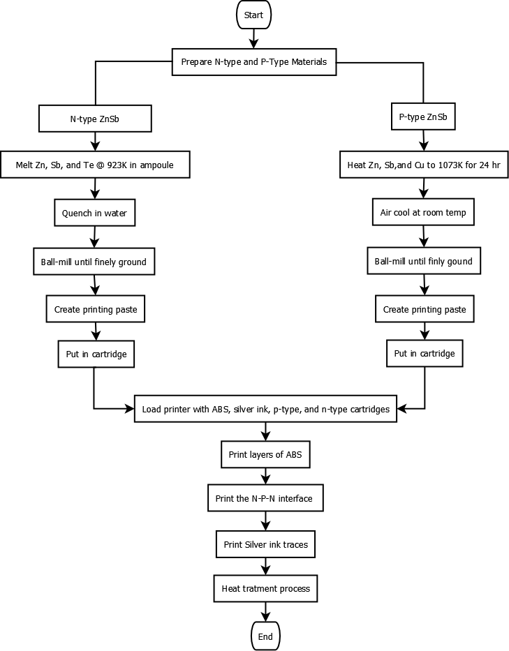
Once the flat surface is achieved the ZnSb semiconductor can be applied to create the semiconductor N-P-N junction. Additionally silver ink[2] may be applied to create conductive traces to carry the signals to and from the transistor. Both the silver ink and the transistor material will need to be cured after application. One possible method of curing the material is the use of a small radiant heating element fitted to the extrusion carriage so that the heat may be applied only where desired to avoid unnecessary thermal input back into the previously extruded material.
After the thermal treatment of the material several additional coatings of polyurethane may be applied to protect the circuit traces and the transistor junction itself. In much the same way that traditional printed circuit boards use vias to provide electrical connection between layers, portions of the circuit may be "masked" off to allow for an electrical equivalent. In places where it is desired to provide interconnection between layers the polyurethane may be excluded during the recoating process.
After the new layer is applied an additional transistor and circuit traces may be applied to increase the density of electrical components within the device. The limitation here is the possibility of electrical interference from adjacent layers due to induced signals from one layer to the next. This along with concerns of dissipating thermal energy will require some ingenuity and experimentation on the part of the daring user.
Materials[edit | edit source]
Cost[edit | edit source]
| Material | Source | Cost | MSDS |
| Zinc | ScienceLab | $0.32/g | [1] |
| Antimony | [2] | $2.19/g | [3] |
| α-terpineol | ScienceLab | $0.20/ml | [4] |
| DisperBYK-110 | BYK | TBA | TBA |
| Copper Granular | ScienceLab | $0.71/g | [5] |
| Tellurium Powder | ScienceLab | $1.57/g | [6] |
| Conductive Silver Ink | iimak | TBA | [7] |
| Verowhite polyeurathane | Redeye | TBA | [8] |
Steps of Synthesizing[edit | edit source]
P-Type ZnSb[edit | edit source]
Doping the ZnSb with copper will create a p-type material. To do this a combination of heating, quenching, and ball-mill crushing will be implemented. All the granular metals (Zinc, Antimony, and Copper) will be together in a container and placed in a furnace. With the furnace set at 1073K for 24 hours, with the occasional rocking. The granular pieces after the furnace will be left to cool at room temperature. Using a ball-milling machine with an argon atmosphere for 1-1.5 hours to finely crush the granulars, similar to the process in.[3] The atomic weight percent of copper needed to have efficient doping is 0.1 at%, as carrier concentration is a diminishing return as copper concentration increases.[3] To get a printable viscosity a process similar to,[4] for this we will use the chemicals α-terpineol and DisperBYK-110 which are the same as.[3] For every 10 grams crushed ZnSb 10 milliliters of α-terpineol will be used and 1 milliliter of DisperBYK-110 and make sure that it is mixed well.
N-Type ZnSb[edit | edit source]
Doping the ZnSb with Tellurium will create an n-type material. To get an n-type ZnSb is very difficult, but can be done. A study,[5] shows that there has to be a certain atomic weight percent of Tellurium, which is 2.06at%. The process of creating the n-type ZnSb is to heat the the granular Zinc and Antimony with the powdered Tellurium at 923 in an ampoule then water quenching the ampoule. After opening the ampoule the materials will be ball-milled until finely crushed After the doping process the process for the P-Type ZnSb paste will be repeated with the α-terpineol at 10 milliliters get 10 grams of ZnSb and the 1 milliliter of DisperBYK-110.
Dia Workflow[edit | edit source]
Purification Methods[edit | edit source]
The raw materials purchased from ScienceLab.com are of acceptable minimum purity for the purpose of creating transistors. The minimum purity for each metal going into the semiconductor is listed in the table below.
| Metal | Purity |
|---|---|
| Zinc | 99.8% (min) |
| Antimony | 99% (min) |
| Copper | 98% (approx) |
| Tellurium | 99.5% (min) |
Testing[edit | edit source]
As a method of testing the doping concentration of tellurium in the n-type zinc antimonide, a wafer is printed. It is then tested to find resistivity using a Signatone Manual Four Point Resistivity Probing Equipment fitted with an SP4 Four Point Probe Head.[6] Resistivity is used to find the doping density according to the following equation:[7]
Where the inverse of the resistivity is , conductivity, e is the charge of an electron, is the electron mobility, and is the donor atom doping concentration.
The p-type ZnSb doping concentration can be determined using a similar method:
Where the inverse of resisitivity is again ,conductivity, e is the charge of a hole (same as the charge of an electron), is the hole mobility, and is the acceptor atom doping concentration.
Material Properties[edit | edit source]
N-type ZnSb[edit | edit source]
- High ZnSb purity (post thermal curing)
- Tellurium concentration: 2.06 at%
- Homogeneous tellurium distribution
P-type ZnSb[edit | edit source]
- High ZnSb purity (post thermal curing)
- Copper concentration: ~0.1 at%
- Homogeneous copper distribution
Characterization[edit | edit source]
One method for characterization of the material is X-ray Diffraction. In this method, x-rays are focused on the material, causing electrons in the material to emit x-rays. These emitted x-rays interfere with each other, either eliminating or intensifying the received x-rays. This intensity depends on the of the angle of the x-ray tube to the sample. The angles that cause x-rays to be emitted depend on the crystal structure. Thus by measuring the intensities at different angles, constants for the crystal structure such as inter-plainer spacing and lattice parameters can be determined. XRD can also be used to indicate point defects.[8]
Another method of characterization is Photoluminescence spectroscopy. This is a non-destructive method of measuring the electrical properties of the semiconductor. Light is focused onto the semiconductor. This light is absorbed through "photo-excitation," forcing the electrons into excited energy states; as the electrons move back to their equilibrium states, they release energy in the form of light equal to the difference between the two energy levels. This light can be detected and measured. Photoluminescence spectroscopy can be used to determine band gaps, impurity levels, and recombination mechanisms.[8]A similar method to photoluminescence spectroscopy is cathodoluminescence spectroscopy, which uses electrons instead of light to excite the material.[8]Because these methods are non-destructive, they are good choices for in-sit characterization.
Applications[edit | edit source]
The beauty behind the 3-D printer is its flexibility and its ability to create nearly any shape from a computer generated geometry file. This already allows for countless possibilities for use in the home. Now add in the ability to print transistors. Modern homes are already full of electronics, and nearly every one of them uses transistors. The simple power to print transistors to replace or modify parts of these electronics is noticeable.
If transistors are able to be printed, then it should be possible to print integrated circuits. With the ability to print chips in the home, anyone with the knowledge could create:
- radios
- remote controllers
- simple memory/storage devices
- simple computer/calculator parts
- and more and more
The ability to print transistors in the home combined with open source designs offers many opportunities for the exploring enthusiast and the practical homeowner alike to expand the foreseeable horizon of applications.
OpenSCAD[edit | edit source]
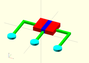
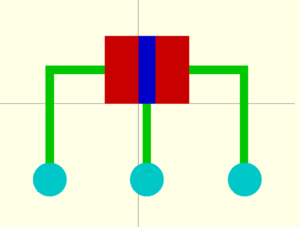
The proposed semiconductor was drawn up using OpenSCAD. The basic design is that of a fairly simple NPN junction.[9] Implementation in real devices will likely require some experimentation on the part of the the end user to determine the optimal scaling of the device based on intended use.
In the two views of the device, the blue material corresponds to the p-type material, the red corresponds to the n-type material. The green sections are conductive traces intended to be made from a material capable of carrying a signal such as Xerox's Silver nano-particle ink[10] The teal circles are locations where the lead may be terminated to a contact or treated as a via to pass between different layers for increased device complexity options.

OpenSCAD:Coding[edit | edit source]
Below is the OpenSCAD code used to generate the model:
//P-type
color([0,0,1])
cube([1,4,1]);
//RH-N-type
color([1,0,0])
translate([1,0,0])
cube([2,4,1]);
//LH-N-type
color([1,0,0])
translate([-2,0,0])
cube([2,4,1]);
//P-contact trace
union(){
color([0,1,0])
translate([0.25,-4,0])
cube([0.5,4,0.5]);
color([0,1,1])
translate([0.5,-4.5,0])
cylinder(h=0.5,r=1,$fn=100);
}
//RH-N-contact trace
union(){
color([0,1,0])
translate([3,1.75,0])
cube([3,0.5,0.5]);
color([0,1,0])
translate([6,-3.75,,0])
cube([0.5,6,0.5]);
color([0,1,1])
translate([6.3,-4.5,0])
cylinder(h=0.5,r=1,$fn=100);
}
//LH-N-contact trace
union(){
color([0,1,0])
translate([-5.0,1.75,0])
cube([3,0.5,0.5]);
color([0,1,0])
translate([-5.5,-3.75,,0])
cube([0.5,6,0.5]);
color([0,1,1])
translate([-5.25,-4.5,0])
cylinder(h=0.5,r=1,$fn=100);
OpenSCAD:STL Modeling[edit | edit source]
The link listed below is for the resulting.stl file for inclusion of the transistor in an actual device. Please note however that the model is scaled quite large using (mostly) integer sizes (mm) so that it can be readily scaled down depending on the application. Scale can be readily applied using the scaling function within OpenSCAD.
Please see the description listed in the OpenSCAD section for material placements & types.
References[edit | edit source]
- ↑ http://www.allaboutcircuits.com/vol_3/chpt_4/1.htmlpdf
- ↑ "Silver Ink to print Plastic Circuits". Xerox Corporation.
- ↑ 3.0 3.1 3.2 http://onlinelibrary.wiley.com/doi/10.1002/pssa.201127211/pdf
- ↑ http://www.sciencedirect.com/science/article/pii/S0040609011006778
- ↑ http://www.jim.or.jp/journal/e/pdf3/50/10/2473.pdf
- ↑ LucasLabs.com: Signatone
- ↑ S.O. Kasap. Principles of Electronic Materials and Devices, Third Edition, McGraw Hill, New Delhi, 2006, p. 389
- ↑ 8.0 8.1 8.2 Razeghi, Manijeh. Fundamentals of Solid State Engineering. Springer US, 2009. Web. https://link.springer.com/chapter/10.1007/978-0-387-92168-6_16=
- ↑ "Bipolar Junction transistor". Wikipedia Bipolar Transistors.
- ↑ "Silver Ink to print Plastic Circuits". Xerox Corporation.
