

Quantum dots (QD) are nanoparticles comprised of semiconductor materials, which exhibit enhanced electronic properties over bulk materials. These properties are defined by a highly adjustable structure of the quantum dot that yields enormous potential in many applications, including photovoltaic cells.[2] A solar cell (also called a photovoltaic cell) is an electrical device that converts the energy of light directly into electricity by the photovoltaic effect. It is a form of photoelectric cell (in that its electrical characteristics—e.g. current, voltage, or resistance—vary when light is incident upon it) which, when exposed to light, can generate and support an electric current without being attached to any external voltage source.[3] If combined with a quantum dot, a high quantum efficiency (percentage of photons transformed into current) is produced, generating a usable total efficiency.[4]The viability of dissolving these quantum dots into a suitable ink for 3-D printing onto a universal solar cell and its processes are analyzed and discussed.
Quantum dot solar cells are often made by depositing quantum dots on thin film ceramics.[5]
3-D Printed Device[edit | edit source]

The scope of this project focuses on photovoltaic cells utilizing CdSe and PbS quantum dots to convert photon energy into current. This particular solar cell will consist of three layers: a p-type (PbS) layer on top; a bulk nano-heterojunction (BNH), or mix of two quantum dots, in the middle; and an n-type (CdSe) layer on the bottom. Each ink will be deposited in layers of.3 mm by the RepRap 3-D printer,[6] with the PbS and BNH consisting of one layer, and the CdSe consisting of two. This method is practical due to the increased n-type doping suggested in BNH devices, as well as the 1:2 p-type to n-type ratio for optimal efficiency.[7] Complete solidification between ink applications may not be necessary, as intermixing between layers may expand the BNH. Carbon nanotubes dispersed throughout the layers will enhance the conductivity of both quantum dots. to work in a low temperature extruder
The optimal matrix for quantum dots and single wall carbon nanotubes (SWNT's) is ABS (Acrylonitrile butadiene styrene), due to its wide array of 3-D printing applications. ABS infused with SWNT exhibits an good electrical conductivity and reduces the normal resistance of 104 ohm-cm considerably. It also exhibits a low printing temperature (about 220° C) without sacrificing solar cell properties, such as composition retention in direct sunlight due to extended exposure. However, ABS has a tendency to crack during application, so a hot plate (of about 110° C) will be supplied to alleviate this issue.[8]
Materials and Processing[edit | edit source]
Every necessary semiconductor material is listed below, with the assumption of purchasing every item; therefore, chemicals used for the synthesis of the listed materials are excluded. A brief description stating the positive properties of each included material is also given.
| Material | Amount Needed | Price | MSDS | Description |
|---|---|---|---|---|
| CdSe/ZnS Core/Shell Amine Coated Quantum Dot | 22.5 mg | $1,161.00/50 mg. | MSDS | n-type semiconductor, adjustable size, great efficiency potential, low thermal conductivity, visible light absorbant |
| PbS/CdS Core/Shell Amine Coated Quantum Dot | 37.5 mg | $1,045.00/25 mg. | MSDS | p-type semiconductor, adjustable size, infrared absorbant |
| C (nanotube, SW) | 0.2 g | $280/1 g. | MSDS | Great electrical conductivity, good surface area, high melting point, outstanding tensile strength |
| ABS filament w/ C (Black), C (fiber), and permanent masterbatch | 2.05 g | $19.95/113.4 g. | MSDS | 3-D printable, high machinability, relatively high strength, ductility, and melting point |
The total cost of all materials was calculated to be $2,505.95, and the quantity of each listed material is one.
Ink Synthesis[edit | edit source]
Sites have been found that would allow the purchase of QD's, ABS, and SWNT's. It can be seen from NOM corp's website that the CdSe QD's absorb light between 500-600nm, which takes care of most of the visible light spectrum. The Dia graphic describes how QD's could be synthesized at home. Synthesizing the dots would require flasks, a glove box, and a great deal of chemicals.
The semiconductor will be made using 3 separate inks: a PbS ink, a CdSe ink, and a mixed ink. All of these inks should have 1x10¹⁶ QD's per cm3 and 100 mg/L of SWNT's.[9][10] Based on these concentrations and a print volume that was determined to be 1.95 cm3, the necessary quantities of each material is given in the 'Amount Needed' column of the bill of materials. This process will require a hopper, a heater, a screw extruder, and a mold. The synthesis process of each ink can be summarized with these steps:
- The ABS will be melted at 250° C.
- The melted ABS and appropriate concentrations of QD's and SWNT's will be mixed in a hopper.
- The liquid ink will be extruded in a mold with the same dimension (1.75 mm diameter) as before.
The complete process is displayed in Figure 3 (right). Figure 3 also outlines the basic steps to prepare and 3-D print CdSe and PbS quantum dots. Detailed information of these two semiconductors is shown below in the bill of materials.
-
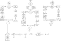
Fig. 3: General Process for 3-D printing CdSe and PbS quantum dots as thin film solar cells
-
![Fig. 4: Cadmium selenide quantum dot synthesis[11]](/w/images/thumb/8/8d/CdSe_QD_Synthesis.png/86px-CdSe_QD_Synthesis.png)
Fig. 4: Cadmium selenide quantum dot synthesis[11]
-
![Fig. 5: Rapid synthesis of PbS colloidal quantum dots[12]](/w/images/thumb/a/ab/PbS_QD_Synthesis.png/78px-PbS_QD_Synthesis.png)
Fig. 5: Rapid synthesis of PbS colloidal quantum dots[12]

![Fig. 4: Cadmium selenide quantum dot synthesis[11]](/File:CdSe_QD_Synthesis.png)
![Fig. 5: Rapid synthesis of PbS colloidal quantum dots[12]](/File:PbS_QD_Synthesis.png)
Purification[edit | edit source]
There are many methods to process - and therefore purify - the PbS quantum dot. With the method described in the PbS synthesis flowchart, the purification phase occurs during the centrifugation process of the raw PbS quantum dot. Ethanol and n-hexane were injected into the system before the centrifuge began, and this entire process was repeated three times. Following this procedure yields high purity quantum dots, as can be seen due to the lack of impurity lines on the x-ray diffraction spectrum.[12]
Another, quicker method has also been used for CdSe, PbSe, and CdTe quantum dots that have been synthesized using oleic acid and octadecene, among other chemicals. By putting the solution that the QD's have been synthesized in into 1.5 of the equivalent amount of acetone and applying a 500 V DC potential across the solution, the QD's will collect at the anode. These can then be rinsed with more acetone for further purification. This is a very quick way to purify quantum dots and has an almost 100% returning yield of nanoparticles.[13]
Testing[edit | edit source]
Ideal Semiconductor Ink Properties[edit | edit source]
This ink is mostly focused on extending the lifetime of charge carriers in the semiconductor. However, another factor that should be considered in the making of this ink, as in all photovoltaic cells, is the range and efficiency of the absorption of photons. These properties will help increase the efficiency of the ink.
- Homogenous distribution of carbon nanotubes among the quantum dots will help conduct improve its ability to act as a charge acceptor.
- Homogenous distribution of the quantum dots allows for more efficient use of the surface area.
- Intermixing of the p-type and n-type QD's in the middle layer to allow a greater interfacial area for diffusion to occur to the junction before recombination occurs within the p- or n-section.[14]
- Range of QD diameters so that a wide range of photon energies can be absorbed.[15]
- Thin layers.
In-Situ Analysis[edit | edit source]
This process takes the trouble of melting and re-solidifying the ABS in a form compatible with the low temperature extruder before 3-D printing the ink. This allows us to perform in-situ analysis on the ink before it is printed.
To test the homogeneity of the quantum dots within the ABS, it would be useful to section off some of the semiconductor ink and take an SEM (scanning electron microscope) image of the section. A coating of chromium or graphite may need to be applied if the ink is not conductive enough.[16] This in-situ analysis would allow the mixing of the QD's to be tested before they are printed out as a solar cell. Also, if a range of QD sizes are observable within the solidified ink, it follows that a range of photon energies will be able to be absorbed.
If the ink is not suitably homogenous, the ABS ink can be remelted and remixed, possibly at a higher temperature to increase solubility. This in-situ analysis can be repeated until the ink is suitably homogenous.
Post-fabrication Testing[edit | edit source]

High-Resolution Transmission Electron Microscopy (HRTEM)
HRTEM is a powerful tool for analysis of properties of materials on the atomic scale.[18] At present, the highest point resolution realized in phase contrast TEM is around 0.5 ångströms (0.050 nm). Phase contrast TEM enables high resolution imaging.[18] This is ideal for semiconductors and in this case, a quantum dot solar cell because individual atoms of a crystal and its defects can be found. Another very important aspect of this analysis is that size of particles can be measured, as well as their distribution. Other uses of this method are:
- Light microscopy using the different refractive indices for differing structures[19]
- X-ray imaging with diffraction contrast through Bragg scattering
- Elemental composition analysis based on unique electron energies
Description of procedure:[20]
- Gloves will be worn whenever handling sample or holders.
- Sample will be prepped for operation.
- After sample is loaded, the microscope will be brought to operating conditions slowly.
- The condenser lens, objective lenses, voltage and current centers will be aligned.
- The accelerating voltage will be reached and an electron beam will be generated.
- Testing until satisfaction and then sample will be removed.
Optical Absorption
When a light is shining on a semiconductor sample, if the energy of the individual photons is greater than the semiconductor band gap, then the photons can be absorbed, transferring their energy to an electron. This is the basis behind optical absorption.[21] The light shined on the sample will be transmitted and then measured by a photodetector. By observing the wavelength at which the sample begins to absorb the light, the bandgap of the sample can be determined. Light incident, reflected, transmitted or scattered by the sample or holder will be absorbed, thus accuracy is important. Intensity of light absorbed can be measured, the fraction of light reflected can be measured, and transmissivity can be measured to yield information about the sample.[21] This information can be complied to gain an idea of how effective a solar cell is.
Discussion[edit | edit source]
3-D Printing Applications[edit | edit source]

Everyone has already seen the old calculators that use solar cells to help power them. It's quite probable that in the future many smart phones, tablets, and other user devices will run on solar power as well. Our application uses a material that many believe will greatly improve solar cell efficiency, quantum dots, as the solar cell semiconductor for these consumer devices. 3-D printing is the superior way to deposit quantum dots onto these devices. Several other techniques are used to deposit quantum dot semiconductors onto surfaces. These include templated assembly and spin casting. However, 3-D printing has an advantage for printing solar cells over both of these deposition techniques.
- The templated assembly requires that a pattern produced by a resist be placed on the substrate where the QD's are supposed to go. This allows for very precise placement of QD's, but is usually only used if one type of QD is to be deposited.[22] For solar cells using a p-type and an n-type layer, putting a resist on top of the bottom layer may disrupt the properties of the interface between the layers.
- Spin casting, on the other hand, allows for multiple layers, such as QD's and graphene, to be deposited on substrate, but it lacks precision.[23] Spin casting uses a flat wheel spinning rapidly to distribute the solution uniformly across the surface of the substrate. It does not allow for depositing around designs or across surfaces that are not extremely flat.
The watch design displayed in the OpenScad shows the advantages of 3-D printing a small photovoltaic cell using QD's. It allows for different design choices to be made, such as the holes for separate dials in the watch, while still depositing layers evenly across the surface. It also allows for multiple layers, which a photovoltaic cell requires, to be deposited. Some limits are still in place before user devices will be a reasonable place to use this application. Lead and cadmium are a heavy metals, which are disapproved of in society for consumer products due to their toxicity to people and environments.[24] Also, these cells could improve in efficiency by reducing thickness. However, quantum dot materials and 3-D printing layer thickness are sure to improve in the future, making this a very powerful application.
Work on quantum dots done by the National Renewable Energy Laboratory (NREL) in Boulder, Colorado has allowed quantum dots to generate more than one electron-hole pair for every photon absorbed. This process is known as multiple exciton generation. It is achieved by incorporating the quantum dots "inside" the solar cell as opposed to being on the surface.[25] This provides an advantage over conventional solar cells as there is less waste energy when light is absorbed.
The stl file for the watch face is below:
https://www.appropedia.org/File:Watch_Face_STL.stl


Code for wrist watch:
translate ([0,0,-3.005])
{color ("Black",1) cylinder (h = 3.5, r=25, $fn=100);}

// cutting into the first 2 layers (CdSe)

difference() {

translate ([0,0,.5])
{color ("Crimson",1) cylinder (h = 1.5, r=25, $fn=100);}
translate ([0,7,1])
{color ("Crimson",1) circle (6.5, $fn=50); }

translate ([7.25,-5.5,1])
{color ("Crimson",1) circle (6.5, $fn=50); }

translate ([-7.25,-5.5,1])
{color ("Crimson",1) circle (6.5, $fn=50) ; }

}

// cutting into the mixed layer (CdSe + PbS)

difference() {

translate ([0,0,2])
{color ("DarkRed",1) cylinder (h = 1, r=25, $fn=100);}
translate ([0,7,1.995])
{color ("DarkRed",1) cylinder (h = 1.5, r=6.7, $fn=50);}

translate ([7.25,-5.5,1.995])
{color ("DarkRed",1) cylinder (h = 1.5, r=6.7, $fn=50);}

translate ([-7.25,-5.5,1.995])
{color ("DarkRed",1) cylinder (h = 1.5, r=6.7, $fn=50);}

}

// cutting into the final layer (PbS)

difference() {

translate ([0,0,3])
{color ("Grey",1) cylinder (h = 1, r=25, $fn=100);}
translate ([0,7,2.995])
{color ("Grey",1) cylinder (h = 1.5, r=6.9, $fn=50);}

translate ([7.25,-5.5,2.995])
{color ("Grey",1) cylinder (h = 1.5, r=6.9, $fn=50);}

translate ([-7.25,-5.5,2.995])
{color ("Grey",1) cylinder (h = 1.5, r=6.9, $fn=50);}

}

translate ([1,17,1])
{color ("Gold",1) cube([1,6,4]); }

translate ([-1,17,1])
{color ("Gold",1) cube([1,6,4]); }

translate ([-23,0,1])
{color ("Gold",1) cube([6,1,4]); }

translate ([0,-23,1])
{color ("Gold",1) cube([1,6,4]); }

translate ([17,0,1])
{color ("Gold",1) cube([6,1,4]); }

rotate([0,0,60]) translate ([17,0,1])
{color ("Black",1) cube([6,1,4]); }

rotate([0,0,30]) translate ([17,0,1])
{color ("Black",1) cube([6,1,4]); }

rotate([0,0,120]) translate ([17,0,1])
{color ("Black",1) cube([6,1,4]); }

rotate([0,0,150]) translate ([17,0,1])
{color ("Black",1) cube([6,1,4]); }

rotate([0,0,210]) translate ([17,0,1])
{color ("Black",1) cube([6,1,4]); }

rotate([0,0,240]) translate ([17,0,1])
{color ("Black",1) cube([6,1,4]); }

rotate([0,0,300]) translate ([17,0,1])
{color ("Black",1) cube([6,1,4]); }

rotate([0,0,330]) translate ([17,0,1])
{color ("Black",1) cube([6,1,4]); }

translate ([0,-1.5,0])
{color ("White",1) cylinder (h = 6, r=1, $fn=50);}

rotate([0,0,35]) translate ([-1,-2,6])
{color ("White",1) cube([14,1.5,1]); }

rotate([0,0,270]) translate ([1,-.5,6])
{color ("White",1) cube([18,1.5,1]); }

rotate([0,0,120]) translate ([-1,.5,6])
{color ("White",1) cube([22,.5,1]); }

// small circles

rotate([0,0,0]) translate ([0,4,1])
{color ("White",1) cube([.5,6,.5]); }

rotate([0,0,0]) translate ([-2.75,6.75,1])
{color ("White",1) cube([6,.5,.5]); }

rotate([0,0,235]) translate ([-.25,6,1])
{color ("White",1) cube([.5,6,.5]); }

rotate([0,0,235]) translate ([-2.75,8.75,1])
{color ("White",1) cube([6,.5,.5]); }

rotate([0,0,135]) translate ([.5,6,1])
{color ("White",1) cube([.5,6,.5]); }

rotate([0,0,135]) translate ([-2.25,8.75,1])
{color ("White",1) cube([6,.5,.5]); }
References[edit | edit source]
- ↑ page.html Solarcellcentral October 11, 2013.
- ↑ Wikipedia: Quantum Dot October 16, 2013
- ↑ Solar Cell - Wikipedia October 11, 2013
- ↑ Wikipedia: Quantum Dot Solar Cell October 16, 2013.
- ↑ QD solar cell company October 15, 2013
- ↑ RepRap layer thickness October 10, 2013
- ↑ BNH ratio October 10, 2013
- ↑ ABS specs October 10, 2013
- ↑ QD concentration October 10, 2013
- ↑ SWNT concentration October 14, 2013
- ↑ Cadmium selenide quantum dot synthesis October 16, 2013.
- ↑ 12.0 12.1 [1] October 16, 2013.
- ↑ Quick purification of QD's October 16, 2013
- ↑ BNH interface October 14, 2013
- ↑ Diameter and absorption October 6, 2013
- ↑ SEM info October 14, 2013
- ↑ gap October 16, 2013
- ↑ 18.0 18.1 [2] October 16, 2013
- ↑ [3] October 16, 2013
- ↑ [4] October 16, 2013
- ↑ 21.0 21.1 [5] October 16, 2013
- ↑ Templated assembly of CdSe October 6, 2013
- ↑ Spin casting with QD's and graphene October 6, 2013
- ↑ Health effects of heavy metals October 16, 2013
- ↑ [ http://solarcellcentral.com/solar_page.html Quantum dot research] October 16, 2013